EVAL-AD7741/42EBZ Analog Devices Inc, EVAL-AD7741/42EBZ Datasheet
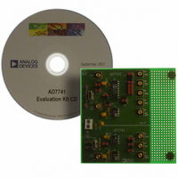
BOARD EVAL FOR AD7741/7742

EVAL-AD7741/42EBZ

Manufacturer Part Number
EVAL-AD7741/42EBZ
Description
BOARD EVAL FOR AD7741/7742
Manufacturer
Analog Devices Inc
Datasheet

Specifications of EVAL-AD7741/42EBZ

Main Purpose
Interface, Voltage to Frequency
Embedded
No
Utilized Ic / Part
AD7741, AD7742
Primary Attributes
2 Devices: 1st with a Single Ended Inputs 0~2.5 V, 2nd with 2 Differential Inputs 0~3.5 V
Secondary Attributes
3072kHz Full Scale, Internal/External Reference Option
Lead Free Status / RoHS Status
Lead free / RoHS Compliant
a
Information furnished by Analog Devices is believed to be accurate and
reliable. However, no responsibility is assumed by Analog Devices for its
use, nor for any infringements of patents or other rights of third parties
which may result from its use. No license is granted by implication or
otherwise under any patent or patent rights of Analog Devices.
GENERAL DESCRIPTION
The AD7741/AD7742 are a new generation of synchronous
voltage-to-frequency converters (VFCs). The AD7741 is a
single-channel version in an 8-lead package (SOIC/DIP) and the
AD7742 is a multichannel version in a 16-lead package (SOIC/
DIP). No user trimming is required to achieve the specified
performance.
The AD7741 has a single buffered input whereas the AD7742
has four buffered inputs that may be configured as two fully-
differential inputs or three pseudo-differential inputs. Both parts
include an on-chip +2.5 V bandgap reference that provides the
user with the option of using this internal reference or an exter-
nal reference.
REV. 0
FEATURES
AD7741: One Single-Ended Input Channel
AD7742: Two Differential or Three Pseudo-Differential
Integral Nonlinearity of 0.012% at f
Single +5 V Supply Operation
Buffered Inputs
Programmable Gain Analog Front-End
On-Chip +2.5 V Reference
Internal/External Reference Option
Power Down to 35 A Max
Minimal External Components Required
8-Lead and 16-Lead DIP and SOIC Packages
APPLICATIONS
Low Cost Analog-to-Digital Conversion
Signal Isolation
Input Channels
(AD7742) and at f
OUT
(Max) = 1.35 MHz (AD7741)
OUT
(Max) = 2.75 MHz
Single and Multichannel, Synchronous
Voltage-to-Frequency Converters
The AD7741 has a single-ended voltage input range from 0 V
to REFIN. The AD7742 has a differential voltage input range
from –V
supply consuming typically 6 mA, and also contain a power-
down feature that reduces the current consumption to less than
35 A.
One Technology Way, P.O. Box 9106, Norwood, MA 02062-9106, U.S.A.
Tel: 781/329-4700
Fax: 781/326-8703
GAIN
V
V
V
V
IN
IN
IN
IN
A1
A0
1
2
3
4
V
IN
REF
INPUT
MUX
V
to +V
GND
DD
FUNCTIONAL BLOCK DIAGRAMS
V
X1
DD
CLKIN
GENERATION
X1/X2
REF
REFIN/OUT
CLOCK
CLKIN
GENERATION
World Wide Web Site: http://www.analog.com
. Both parts operate from a single +5 V
CLKOUT
VOLTAGE-TO-
MODULATOR
FREQUENCY
CLOCK
UNI/BIP
CLKOUT
VOLTAGE-TO-
MODULATOR
FREQUENCY
AD7741/AD7742
REFERENCE
+2.5V
AD7742
REFIN
GND
© Analog Devices, Inc., 1999
AD7741
POWER-DOWN
REFOUT
POWER-DOWN
LOGIC
PD
LOGIC
PD
REFERENCE
+2.5V
f
OUT
f
OUT

Related parts for EVAL-AD7741/42EBZ

EVAL-AD7741/42EBZ Summary of contents

Page 1

FEATURES AD7741: One Single-Ended Input Channel AD7742: Two Differential or Three Pseudo-Differential Input Channels Integral Nonlinearity of 0.012 (AD7742) and at f (Max) = 1.35 MHz (AD7741) OUT Single +5 V Supply Operation Buffered Inputs Programmable Gain ...

Page 2

AD7741–SPECIFICATIONS 2 Parameter DC PERFORMANCE Integral Nonlinearity 200 kHz CLKIN MHz CLKIN f = 6.144 MHz CLKIN Offset Error Gain Error 3 Offset Error Drift 3 Gain Error Drift 3 Power Supply Rejection ...

Page 3

AD7742–SPECIFICATIONS B Version 3 Parameter Min DC PERFORMANCE Integral Nonlinearity 200 kHz CLKIN MHz CLKIN f = 6.144 MHz CLKIN Offset Error Gain Error +0.2 +0.2 4 Offset Error Drift 4 Gain Error ...

Page 4

AD7741/AD7742 TIMING CHARACTERISTICS Limit at T MIN Parameter (B and Y Version) f 6.144 CLKIN t /t 55/45 HIGH LOW 45/ HIGH NOTES 1 Guaranteed by design ...

Page 5

Pin No. Mnemonic Function 1 V Power Supply Input. These parts can be operated from +4. +5.25 V and the supply should DD be adequately decoupled to GND. 2 GND Ground reference point for all circuitry on the ...

Page 6

AD7741/AD7742 Pin No. Mnemonic Function 1 f Frequency Output. This pin provides the output of the synchronous VFC. OUT 2 V Power Supply Input. These parts can be operated from +4. +5.25 V and the supply should be ...

Page 7

TERMINOLOGY INTEGRAL NONLINEARITY For the VFC, Integral Nonlinearity (INL measure of the maximum deviation from a straight line passing through the actual endpoints of the VFC transfer function. The error is expressed the frequency span: ...

Page 8

AD7741/AD7742 UNI/BIP GAIN Gain, G N/A N can be seen from Table II, the AD7741 has one input range configuration whereas the AD7742 has unipolar/bipolar as ...

Page 9

The digital data that represents the analog input voltage is con- tained in the duty cycle of the pulse train appearing at the out- put of the comparator. The output is a fixed-width pulse whose frequency depends on the analog ...

Page 10

AD7741/AD7742 APPLICATIONS The basic connection diagram for the part is shown in Figure 9. In the connection diagram shown, the AD7742 analog inputs are configured as fully differential, bipolar inputs with a gain quartz crystal provides the ...

Page 11

Isolation Applications In addition to analog-to-digital conversion, the AD7741/AD7742 can be used in isolated analog signal transmission applications. Due to noise, safety requirements or distance, it may be neces- sary to isolate the AD7741/AD7742 from any controlling circuitry. This can ...

Page 12

AD7741/AD7742 8-Lead Plastic DIP (N-8) 0.430 (10.92) 0.348 (8.84 0.280 (7.11) 0.240 (6.10 0.325 (8.25) PIN 1 0.100 (2.54) 0.300 (7.62) BSC 0.060 (1.52) 0.210 0.015 (0.38) (5.33) MAX 0.130 0.160 (4.06) (3.30) MIN 0.115 (2.93) ...

Related keywords