EVAL-ADV7180LFEBZ Analog Devices Inc, EVAL-ADV7180LFEBZ Datasheet
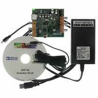
EVAL-ADV7180LFEBZ
Specifications of EVAL-ADV7180LFEBZ
Available stocks


Related parts for EVAL-ADV7180LFEBZ


EVAL-ADV7180LFEBZ Summary of contents
Page 1
FEATURES FEATURES Automotive versions qualified per AEC-Q100, Grade 1 Automotive versions qualified per AEC-Q100, Grade 1 Worldwide NTSC/PAL/SECAM color demodulation support Worldwide NTSC/PAL/SECAM color demodulation support One 10-bit ADC, 4× oversampling for CVBS, 2× oversampling One 10-bit ADC, 4× oversampling ...
Page 2
ADV7180 TABLE OF CONTENTS Features .............................................................................................. 1 Applications ....................................................................................... 1 Functional Block Diagram .............................................................. 1 General Description ......................................................................... 1 Revision History ............................................................................... 3 Introduction ...................................................................................... 4 Analog Front End ......................................................................... 4 Standard Definition Processor ................................................... 4 Comparison with the ADV7181B ...
Page 3
REVISION HISTORY 4/09—Rev Rev. C Changes to Features Section ............................................................ 1 Changes to Absolute Maximum Ratings, Table 7 ....................... 11 Changes to Figure 7 and Table 8, EPAD Addition ...................... 12 Added Power-On RESET Section ................................................. 17 Changes ...
Page 4
ADV7180 INTRODUCTION The ADV7180 is a versatile one-chip multiformat video decoder that automatically detects and converts PAL, NTSC, and SECAM standards in the form of composite, S-video, and component video into a digital ITU-R BT.656 format. The simple digital output ...
Page 5
COMPARISON WITH THE ADV7181B In comparison with the ADV7181B, the 64-lead LQFP ADV7180 has the following additional features: • Improved VCR and weak tuner locking capabilities • Three on-chip antialiasing filters • Four general-purpose outputs (GPOs) • An analog supply ...
Page 6
ADV7180 FUNCTIONAL BLOCK DIAGRAMS XTAL1 XTAL ANALOG VIDEO INPUTS XTAL1 XTAL ANALOG VIDEO INPUTS A 3 ...
Page 7
SPECIFICATIONS Temperature range −40°C to +85°C. The minimum/maximum specifications are guaranteed over this range. MIN MAX ELECTRICAL CHARACTERISTICS VDD VDD ...
Page 8
ADV7180 VIDEO SPECIFICATIONS Guaranteed by characterization VDD specified at operating temperature range, unless otherwise noted. Table 3. Parameter NONLINEAR SPECIFICATIONS Differential Phase Differential Gain Luma Nonlinearity NOISE SPECIFICATIONS SNR Unweighted Analog Front-End Crosstalk LOCK TIME SPECIFICATIONS Horizontal Lock ...
Page 9
TIMING SPECIFICATIONS Guaranteed by characterization VDD specified at operating temperature range, unless otherwise noted. Table 4. Parameter SYSTEM CLOCK AND CRYSTAL Nominal Frequency Frequency Stability PORT SCLK Frequency SCLK Minimum Pulse Width High SCLK Minimum ...
Page 10
ADV7180 TIMING DIAGRAMS t SDATA SCLK OUTPUT LLC OUTPUTS P0 TO P15, VS Figure Timing HS, FIELD, SFL Figure ...
Page 11
ABSOLUTE MAXIMUM RATINGS Table 7. Parameter Rating A to AGND 2.2 V VDD D to DGND 2.2 V VDD P to AGND 2.2 V VDD D to DGND 4 V VDDIO −0 VDDIO ...
Page 12
ADV7180 PIN CONFIGURATIONS AND FUNCTION DESCRIPTIONS 40-LEAD LFCSP Table 8. 40-Lead LFCSP Pin Function Descriptions Pin No. Mnemonic Type 1, 4 DVDDIO P 2 SFL O 3, 15, 35, 40 DGND 10, 16 P2, ...
Page 13
LQFP INTRQ DGND DVDDIO DGND DVDDIO GPO1 GPO0 CONNECT Table 9. 64-Lead LQFP Pin Function Description Pin No. Mnemonic Type 1 INTRQ 10, 24, 57 DGND DVDDIO P ...
Page 14
ADV7180 Pin No. Mnemonic Type 38 VREFP O 39 VREFN O 40 AVDD P 51 RESET I 52 ALSB I 53 SDATA I/O 54 SCLK I 63 FIELD Description Internal Voltage Reference Output. See Figure 54 ...
Page 15
ANALOG FRONT END MAN_MUX_EN MUX_0[3: MUX_1[3: ...
Page 16
ADV7180 INPUT CONFIGURATION The following are the two key steps for configuring the ADV7180 to correctly decode the input video: 1. Use INSEL[3:0] to configure the routing and format decoding (CVBS, Y/C, or YPrPb). For the 64-lead LQFP, see Table ...
Page 17
POWER-ON RESET After power-up necessary to execute a reset operation. For correct operation, RESET should remain deasserted for 5 ms after power supplies are stable and within specification and PWRDWN is asserted. ANALOG INPUT MUXING The ADV7180 has ...
Page 18
ADV7180 ANTIALIASING FILTERS The ADV7180 has optional on-chip antialiasing (AA) filters on each of the three channels that are multiplexed to the ADC (see Figure 12). The filters are designed for standard definition video MHz bandwidth. Figure ...
Page 19
GLOBAL CONTROL REGISTERS Register control bits listed in this section affect the whole chip. POWER-SAVING MODES Power-Down PDBP, Address 0x0F[2] The digital supply of the ADV7180 can be shut down by using the PWRDWN pin or via ...
Page 20
ADV7180 Timing Signals Output Enable TIM_OE, Address 0x04[3] The TIM_OE bit should be regarded as an addition to the TOD bit. Setting it high forces the output drivers for HS, VS, and FIELD into the active state (that is, driving ...
Page 21
GLOBAL STATUS REGISTER Four registers provide summary information about the video decoder. The IDENT register allows the user to identify the revision code of the ADV7180. The other three registers (0x10, 0x12, and 0x13) contain status bits from the ADV7180. ...
Page 22
ADV7180 VIDEO PROCESSOR STANDARD DEFINITION PROCESSOR MACROVISION DETECTION DIGITIZED CVBS LUMA DIGITIZED Y (YC) DIGITAL FINE CLAMP DIGITIZED CVBS CHROMA DIGITIZED C (YC) DIGITAL CHROMA FINE DEMOD CLAMP RECOVERY Figure 15 shows a block diagram of the ADV7180 video processor. ...
Page 23
SYNC PROCESSING The ADV7180 extracts syncs embedded in the analog input video signal. There is currently no support for external HS/VS inputs. The sync extraction is optimized to support imperfect video sources, such as VCRs with head switches. The actual ...
Page 24
ADV7180 AD_SECAM_EN, Enable Autodetection of SECAM, Address 0x07[6] Setting AD_SECAM_EN to 0 (default) disables the autodetection of SECAM. Setting AD_SECAM_EN to 1 enables the detection of SECAM. AD_N443_EN, Enable Autodetection of NTSC 4.43, Address 0x07[5] Setting AD_N443_EN to 0 disables ...
Page 25
... Using the SRLS bit, the user can choose between two sources for determining the lock status (per Bits[1:0] in the Status 1 Register). Refer to Figure 16. • The TIME_WIN signal is based on a line-to-line evaluation of the horizontal synchronization pulse of the incoming video. It reacts quite quickly. • ...
Page 26
ADV7180 SD_SAT_Cr[7:0], SD Saturation Cr Channel, Address 0xE4[7:0] This register allows the user to control the gain of the Cr channel only, which in turn adjusts the saturation of the picture. Table 26. SD_SAT_Cr Function SD_SAT_Cr[7:0] Description 0x80 (default) Gain ...
Page 27
DEF_VAL_AUTO_EN, Default Value Automatic Enable, Address 0x0C[1] This bit enables the automatic use of the default values for Y, Cr, and Cb when the ADV7180 cannot lock to the video signal. Setting DEF_VAL_AUTO_EN to 0 disables free-run mode. If the ...
Page 28
ADV7180 DCT[1:0], Digital Clamp Timing, Address 0x15[6:5] The clamp timing register determines the time constant of the digital fine clamp circuitry important to note that the digital fine clamp reacts quickly because it immediately corrects any residual dc ...
Page 29
... An automatic mode is provided that allows the ADV7180 to evaluate the quality of the incoming video signal and select the filter responses in accordance with the signal quality and video standard. YFSM, WYSFMOVR, and WYSFM allow the user to manually override the automatic decisions in part or in full. ...
Page 30
ADV7180 Table 32. YSFM Function YSFM[4:0] Description 00000 Automatic selection including a wide-notch response (PAL/NTSC/SECAM) 00001 (default) Automatic selection including a narrow-notch response (PAL/NTSC/SECAM) 00010 SVHS 1 00011 SVHS 2 00100 SVHS 3 00101 SVHS 4 00110 SVHS 5 00111 ...
Page 31
CHROMA FILTER Data from the digital fine clamp block is processed by the three sets of filters that follow. Note that the data format at this point is CVBS for CVBS inputs, chroma only for Y/C, or U/V interleaved for ...
Page 32
ADV7180 CSFM[2:0], C Shaping Filter Mode, Address 0x17[7:5] The C shaping filter mode bits allow the user to select from a range of low-pass filters for the chrominance signal. When switched in automatic mode, the widest filter is selected based ...
Page 33
Luma Gain LAGC[2:0], Luma Automatic Gain Control, Address 0x2C[6:4] The luma automatic gain control mode bits select the operating mode for the gain control in the luma path. There are internal parameters (Analog Devices proprietary algorithms) to customize the peak ...
Page 34
ADV7180 BETACAM, Enable Betacam Levels, Address 0x01[5] If YPrPb data is routed through the ADV7180, the automatic gain control modes can target different video input levels, as outlined in Table 41. The BETACAM bit is valid only if the input ...
Page 35
CAGT[1:0], Chroma Automatic Gain Timing, Address 0x2D[7:6] The chroma automatic gain timing register allows the user to influence the tracking speed of the chroma automatic gain control. This register has an effect only if the CAGC[1:0] register is set to ...
Page 36
ADV7180 CHROMA TRANSIENT IMPROVEMENT (CTI) The signal bandwidth allocated for chroma is typically much smaller than that of luminance. In the past, this was a valid way to fit a color video signal into a given overall bandwidth because the ...
Page 37
DIGITAL NOISE REDUCTION (DNR) AND LUMA PEAKING FILTER Digital noise reduction is based on the assumption that high frequency signals with low amplitude are probably noise and that their removal, therefore, improves picture quality. The following are the two DNR ...
Page 38
ADV7180 COMB FILTERS The comb filters of the ADV7180 have been greatly improved to automatically handle video of all types, standards, and levels of quality. The NTSC and PAL configuration registers allow the user to customize the comb filter operation ...
Page 39
YCMN[2:0], Luma Comb Mode NTSC, Address 0x38[2:0] Table 53. YCMN Function YCMN[2:0] Description 000 (default) Adaptive comb mode 100 Disable luma comb 101 Fixed luma comb (top lines of line memory) 110 Fixed luma comb (all lines of line memory) ...
Page 40
ADV7180 IF FILTER COMPENSATION IFFILTSEL[2:0], IF Filter Select, Address 0xF8[2:0] The IFFILTSEL[2:0] register allows the user to compensate for SAW filter characteristics on a composite input, as would be observed on tuner outputs. Figure 29 and Figure 30 show IF ...
Page 41
AV CODE INSERTION AND CONTROLS 2 This section describes the I C-based controls that affect the following: • Insertion of AV codes into the data stream • Data blanking during the vertical blank interval (VBI) • The range of data ...
Page 42
ADV7180 BL_C_VBI, Blank Chroma During VBI, Address 0x04[2] Setting BL_C_VBI high blanks the Cr and Cb values of all VBI lines. This is done so any data that may arrive during VBI is not decoded as color and is output ...
Page 43
SYNCHRONIZATION OUTPUT SIGNALS HS Configuration The following controls allow the user to configure the behavior of the HS output pin only: • Beginning of HS signal via HSB[10:0] • End of HS signal via HSE[10:0] • Polarity of HS using ...
Page 44
ADV7180 VS and FIELD Configuration The following controls allow the user to configure the behavior of the VS and FIELD output pins, as well as the generation of embedded AV codes. The 64-lead LQFP has separate VS and FIELD pins. ...
Page 45
PF, Polarity FIELD, Address 0x37[3] The polarity of the FIELD pin for the LQFP part can be inverted using the PF bit. The FIELD pin can be inverted using the PF bit. When (default), FIELD is active ...
Page 46
ADV7180 NVBEGSIGN 1 ADVANCE BEGIN OF VSYNC BY NVBEG[4:0] NOT VALID FOR USER PROGRAMMING ODD FIELD? YES NVBEGDELO ADDITIONAL DELAY BY 1 LINE VSBHO ADVANCE BY 0.5 LINE VSYNC BEGIN Figure 35. NTSC VSYNC ...
Page 47
NVEND[4:0], NTSC VSYNC End, Address 0xE6[4:0] The default value of NVEND is 00100, indicating the NTSC VSYNC end position. For all NTSC/PAL VSYNC timing controls, both the V bit in the AV code and the VSYNC on the VS pin ...
Page 48
ADV7180 622 623 624 625 OUTPUT VIDEO HS OUTPUT VS OUTPUT FIELD OUTPUT 310 311 312 OUTPUT VIDEO HS OUTPUT VS OUTPUT FIELD OUTPUT Figure 39. PAL Typical VS/FIELD Positions Using Register Writes Shown in Table 63 Table 63. User ...
Page 49
PVENDSIGN 1 ADVANCE END OF VSYNC BY PVEND[4:0] NOT VALID FOR USER PROGRAMMING ODD FIELD? YES PVENDDELO ADDITIONAL DELAY BY 1 LINE VSEHO ADVANCE BY 0.5 LINE VSYNC END Figure 41. PAL VSYNC End ...
Page 50
ADV7180 ENHSPLL, Enable HSYNC Processor, Address 0x01[6] The HSYNC processor is designed to filter incoming HSYNCs that have been corrupted by noise, providing improved performance for video signals with stable time bases but poor SNR. Setting ENHSPLL to 0 disables ...
Page 51
Table 66. Default Standards on Lines for PAL and NTSC PAL—625/50 Default VBI Line No. Data Decoded Line No. 6 WST 318 7 WST 319 8 WST 320 9 WST 321 10 WST 322 11 WST 323 12 WST 324 ...
Page 52
ADV7180 Table 68.VBI Data Standards to be Decoded on Line Px (PAL) or Line Ny (NTSC) Signal Name Register Location VBI_DATA_P6_N23 VDP_LINE_00F[7:4] VBI_DATA_P7_N24 VDP_LINE_010[7:4] VBI_DATA_P8_N25 VDP_LINE_011[7:4] VBI_DATA_P9 VDP_LINE_012[7:4] VBI_DATA_P10 VDP_LINE_013[7:4] VBI_DATA_P11 VDP_LINE_014[7:4] VBI_DATA_P12_N10 VDP_LINE_015[7:4] VBI_DATA_P13_N11 VDP_LINE_016[7:4] VBI_DATA_P14_N12 VDP_LINE_017[7:4] VBI_DATA_P15_N13 VDP_LINE_018[7:4] ...
Page 53
VDP_TTXT_TYPE_MAN_ENABLE, Enable Manual Selection of Teletext Type, Address 0x60[2], User Sub Map Setting VDP_TTXT_TYPE_MAN_ENABLE to 0 (default), the manual programming of the teletext type is disabled. Setting VDP_TTXT_TYPE_MAN_ENABLE to 1, the manual programming of the teletext type is enabled. VDP_TTXT_TYPE_MAN[1:0], ...
Page 54
ADV7180 The ancillary data packet sequence is explained in Table 71 and Table 72. The nibble output mode is the default mode of output from the ancillary stream when ancillary stream output is enabled. This format is in compliance with ...
Page 55
Table 72. Ancillary Data in Byte Output Format Byte Padding[1:0] EP ...
Page 56
ADV7180 Data Bytes The VBI_WORD_4 to VBI_WORD_N + 3 contains the data- words that were decoded by the VDP in the transmission order. The position of bits in bytes is in the inverse transmission order. For example, closed captioning has ...
Page 57
I C Interface 2 Dedicated I C readback registers are available for CCAP, CGMS, WSS, Gemstar, VPS, PDC/UTC, and VITC. Because teletext is a high data rate standard, data extraction is supported only through the ancillary data packet. 2 ...
Page 58
ADV7180 The sequence for the interrupt-based reading of the VDP I data registers is as follows for the CCAP standard: 1. The user unmasks the CCAP interrupt mask bit (0x50 Bit 0, user sub map = 1). CCAP data occurs ...
Page 59
I C READBACK REGISTERS Teletext Because teletext is a high data rate standard, the decoded bytes are available only as ancillary data. However, a TTXT_AVL bit 2 has been provided that the user can check ...
Page 60
ADV7180 CGMS and WSS The CGMS and WSS data packets convey the same type of information for different video standards. WSS is for PAL and CGMS is for NTSC; therefore, the CGMS and WSS readback registers are shared. WSS is ...
Page 61
CCAP Two bytes of decoded closed caption data are available in the registers. The field information of the decoded CCAP data can be obtained from the CC_EVEN_FIELD bit (Register 0x78). CC_CLEAR, Closed Caption Clear, Address 0x78[0], User ...
Page 62
ADV7180 VITC VITC has a sequence of 10 syncs in between each data byte. The VDP strips these syncs from the data stream to output only the data bytes. The VITC results are available in Register VDP_VITC_DATA_0 to Register VDP_VITC_DATA_8 ...
Page 63
... The readback registers for VPS, PDC, and UTC are shared. Gemstar is a high data rate standard and is available only through the ancillary stream. However, for evaluation purposes, any one line of Gemstar is available through the I same register space as PDC, UTC, and VPS. Therefore, only ...
Page 64
ADV7180 Table 82. GS/VPS/PDC/UTC Readback Registers Signal Name GS_VPS_PDC_UTC_BYTE_0[7:0] GS_VPS_PDC_UTC_BYTE_1[7:0] GS_VPS_PDC_UTC_BYTE_2[7:0] GS_VPS_PDC_UTC_BYTE_3[7:0] VPS_PDC_UTC_BYTE_4[7:0] VPS_PDC_UTC_BYTE_5[7:0] VPS_PDC_UTC_BYTE_6[7:0] VPS_PDC_UTC_BYTE_7[7:0] VPS_PDC_UTC_BYTE_8[7:0] VPS_PDC_UTC_BYTE_9[7:0] VPS_PDC_UTC_BYTE_10[7:0] VPS_PDC_UTC_BYTE_11[7:0] VPS_PDC_UTC_BYTE_12[7:0] 1 The default value does not apply to readback registers. VBI System 2 The user has an option of ...
Page 65
Each data packet starts immediately after the EAV code of the preceding line. Figure 47 and Table 83 show the overall structure of the data packet. Entries within the packet are as follows: • Fixed preamble sequence of 0x00, 0xFF, ...
Page 66
ADV7180 Gemstar Bit Names The following are the Gemstar bit names: • DID—The data identification value is 0x140 (10-bit value). Care has been taken so that in 8-bit systems, the two LSBs do not carry vital information. • EP and ...
Page 67
Table 86. Gemstar_2× Data, Full-Byte Mode Byte D[9] D[8] D[ CS[8] ...
Page 68
ADV7180 Table 89. NTSC CCAP Data, Half-Byte Mode Byte D[9] D[8] D[ ...
Page 69
Table 91. PAL CCAP Data, Half-Byte Mode Byte D[9] D[8] D[ ...
Page 70
ADV7180 Table 93. NTSC Line Enable Bits and Corresponding Line Numbering Line Number Line[3:0] (ITU-R BT.470) Enable Bit 0 10 GDECOL[ GDECOL[ GDECOL[ GDECOL[ GDECOL[ GDECOL[ GDECOL[6] 7 ...
Page 71
Letterbox Detection Incoming video signals may conform to different aspect ratios (16:9 wide screen or 4:3 standard). For certain transmissions in the wide-screen format, a digital sequence (WSS) is transmitted with the video signal WSS sequence is provided, ...
Page 72
ADV7180 PIXEL PORT CONFIGURATION The ADV7180 has a very flexible pixel port that can be configured in a variety of formats to accommodate downstream ICs. Table 97, Table 98, and Table 99 summarize the various functions that the ADV7180 pins ...
Page 73
GPO CONTROL The 64-lead LQFP has four general-purpose outputs (GPO). These outputs allow the user to control other devices system via the I C port of the 64-lead LQFP. The 40-lead LFCSP does not have GPO pins. ...
Page 74
ADV7180 MPU PORT DESCRIPTION 2 The ADV7180 supports a 2-wire (I C-compatible) serial inter- face. Two inputs, serial data (SDATA) and serial clock (SCLK), carry information between the ADV7180 and the system I master controller. Each slave device is recognized ...
Page 75
REGISTER ACCESS The MPU can write to or read from all of the ADV7180 registers except the subaddress register, which is write only. The subaddress register determines which register the next read or write operation accesses. All communications with the ...
Page 76
ADV7180 REGISTER MAPS Table 102. Main Register Map Details Address Dec Hex Register Name Input Control RW VID_SEL[3] VID_SEL[ Video Selection RW ENHSPLL 3 03 Output Control RW VBI_EN TOD ...
Page 77
Address Dec Hex Register Name 155 9B Letterbox 1 R LB_LCT[7] LB_LCT[6] 156 9C Letterbox 2 R LB_LCM[7] LB_LCM[6] 157 9D Letterbox 3 R LB_LCB[7] LB_LCB[6] 178 B2 CRC Enable W 195 C3 ADC Switch 1 RW ...
Page 78
ADV7180 Table 103. Interrupt System Register Map Details Address Dec Hex Register Name Interrupt Config INTRQ_DUR_ SEL[ Interrupt Status Interrupt Clear Interrupt Mask 1 ...
Page 79
Address Dec Hex Register Name RW 7 118 76 VDP_LINE_020 RW VBI_DATA_ P23_N21[3] 119 77 VDP_LINE_021 RW VBI_DATA_ P24_N22[3] 120 78 VDP_STATUS_ W CLEAR 120 78 VDP_STATUS R TTXT_AVL 121 79 VDP_CCAP_ R CCAP_BYTE_1[7] CCAP_BYTE_1[6] CCAP_BYTE_1[5] CCAP_BYTE_1[4] CCAP_BYTE_1[3] CCAP_BYTE_1[2] CCAP_BYTE_1[1] ...
Page 80
ADV7180 Table 104. Register Map Descriptions (Normal Operation) Subaddress Register Bit Description 0x00 Input Control INSEL[3:0]; the INSEL bits allow the user to select an input channel and the input format; refer to Table 11 and Table 10 for full ...
Page 81
Subaddress Register Bit Description 0x01 Video Selection Reserved SQPE ENVSPROC Reserved BETACAM ENHSPLL Reserved 0x03 Output Control SD_DUP_AV; duplicates the AV codes from the luma into the chroma path Reserved OF_SEL[3:0]; allows the user to choose from a set of ...
Page 82
ADV7180 Subaddress Register Bit Description Reserved Reserved BT.656-4; allows the user to select an output mode compatible with ITU-R BT.656-3/-4 0x05 Reserved 0x06 Reserved 0x07 Autodetect AD_PAL_EN; PAL B/D/I/G/H Enable autodetect enable AD_NTSC_EN; NTSC autodetect enable AD_PALM_EN; PAL M autodetect ...
Page 83
Subaddress Register Bit Description 0x0E ADI Control 1 Reserved SUB_USR_EN; enables user to access the interrupt/ VDP register map Reserved 0x0F Power Mgmt Reserved PDBP; power-down bit priority selects between PWRDWN bit or pin control Reserved PWRDWN; power-down places the ...
Page 84
ADV7180 Subaddress Register Bit Description 0x14 Analog Reserved Clamp Control CCLEN; current clamp enable allows the user to switch off the current sources in the analog front Reserved 0x15 Digital Clamp Reserved Control 1 DCFE; digital clamp freeze enable DCT[1:0]; ...
Page 85
Subaddress Register Bit Description 0x18 Shaping Filter WYSFM[4:0]; wideband Y Control 2 shaping filter mode allows the user to select which Y shaping filter is used for the Y component of Y/C, YPrPb, B/W input signals also used ...
Page 86
ADV7180 Subaddress Register Bit Description 0x27 Pixel Delay LTA[1:0]; luma timing Control adjust allows the user to specify a timing difference between chroma and luma samples Reserved CTA[2:0]; chroma timing adjust allows a specified timing difference between the luma and ...
Page 87
Subaddress Register Bit Description 0x2E Chroma Gain CMG[7:0]/CG[7:0]; chroma Control 2 manual gain lower eight bits; see CMG[11:8]/ CG[11:8] for description 0x2F Luma Gain LMG[11:8]/LG[11:8]; in Control 1 manual mode, luma gain control can be used to program a desired ...
Page 88
ADV7180 Subaddress Register Bit Description 0x36 HS Position HSE[7:0]; see previous Control 3 description 0x37 Polarity PCLK; sets polarity of LLC Reserved PF; sets the FIELD polarity Reserved PVS; sets the VS polarity Reserved PHS; sets HS polarity 0x38 NTSC ...
Page 89
Subaddress Register Bit Description CTAPSP[1:0]; chroma comb taps, PAL 0x3A ADC Control MUX PDN Override; mux power-down override PWRDWN_MUX_2; enables power-down of MUX2 and associated channel clamp and buffer PWRDWN_MUX_1; enables power-down of MUX1 and associated channel clamp and buffer ...
Page 90
ADV7180 Subaddress Register Bit Description 0x48 Gemstar GDECEL[15:8]; see the Comments column Control 1 0x49 Gemstar GDECEL[7:0] Control 2 0x4A Gemstar GDECOL[15:8]; see the Control 3 Comments column 0x4B Gemstar GDECOL[7:0] Control 4 GDECAD; controls the 0x4C Gemstar Control 5 ...
Page 91
... Over field with vertical info 1 Line-to-line evaluation 0 Lock status set only by horizontal lock 1 Lock status set by horizontal lock and subcarrier lock 0 FIELD 1 VSYNC 0 Set to default 0 ADC sampling control 1 Y/C mode only ...
Page 92
ADV7180 Subaddress Register Bit Description 0x9B Letterbox 1 LB_LCT[7:0]; letterbox (Read Only) data register 0x9C Letterbox 2 LB_LCM[7:0]; letterbox (Read Only) data register 0x9D Letterbox 3 LB_LCB[7:0]; letterbox (Read Only) data register 0xB2 CRC Enable Reserved (Write Only) CRC_ENABLE; enable ...
Page 93
Subaddress Register Bit Description 0xDE ST Noise ST_NOISE[10:8] Readback 1 ST_NOISE_VLD (Read Only) 0xDF ST Noise ST_NOISE[7:0] Readback 2 (Read Only) 0xE1 SD Offset Cb SD_OFF_Cb[7:0]; adjusts the hue by selecting the offset for the Cb channel 0xE2 SD Offset ...
Page 94
ADV7180 Subaddress Register Bit Description 0xE7 NTSC F Bit NFTOG[4:0]; number of Toggle lines after l COUNT toggle F signal NFTOGSIGN NFTOGDELE; delay F transition by one line relative to NFTOG (even field) NFTOGDELO; delay F transition by one line ...
Page 95
Subaddress Register Bit Description 0xEB Vblank Control 1 PVBIELCM[1:0]; PAL VBI even field line control PVBIOLCM[1:0]; PAL VBI odd field line control NVBIELCM[1:0]; NTSC VBI even field line control NVBIOLCM[1:0]; NTSC VBI odd field line control 0xEC Vblank Control 2 ...
Page 96
ADV7180 Subaddress Register Bit Description 0xF4 Drive Strength DR_STR_S[1:0]; selects the drive strength for the sync output signals DR_STR_C[1:0]; selects the drive strength for the clock output signal DR_STR[1:0]; selects the drive strength for the data output signals; can be ...
Page 97
Table 105. Register Map Descriptions (Interrupt Operation) User Sub Map Address Register Bit Description 0x40 Interrupt Configuration 1 INTRQ_OP_SEL[1:0]; interrupt drive level select MPU_STIM_INTRQ; manual interrupt set mode Reserved MV_INTRQ_SEL[1:0]; Macrovision interrupt select INTRQ_DUR_SEL[1:0]; interrupt duration select 0x42 Interrupt Status ...
Page 98
ADV7180 User Sub Map Address Register Bit Description 0x45 Raw Status 1 CCAPD (Read Only) Reserved EVEN_FIELD Reserved MPU_STIM_INTRQ 0x46 Interrupt Status 2 CCAPD_Q (Read Only) GEMD_Q Reserved SD_FIELD_CHNGD_Q Reserved Reserved MPU_STIM_INTRQ_Q 0x47 Interrupt Clear 2 CCAPD_CLR (Write Only) GEMD_CLR ...
Page 99
User Sub Map Address Register Bit Description 0x4A Interrupt Status 3 SD_OP_CHNG_Q Hz/50 Hz (Read Only) frame rate at output SD_V_LOCK_CHNG_Q SD_H_LOCK_CHNG_Q SD_AD_CHNG_Q; SD autodetect changed SCM_LOCK_CHNG_Q; SECAM lock PAL_SW_LK_CHNG_Q Reserved Reserved 0x4B Interrupt Clear 3 SD_OP_CHNG_CLR (Write ...
Page 100
ADV7180 User Sub Map Address Register Bit Description 0x4E Interrupt Status 4 (Read Only) VDP_CCAPD_Q Reserved VDP_CGMS_WSS_CHNGD_Q; see 0x9C Bit 4 of user sub map to determine whether interrupt is issued for a change in detected data or for when ...
Page 101
User Sub Map Address Register Bit Description 0x61 VDP_Config_2 Reserved AUTO_DETECT_GS_TYPE Reserved 0x62 VDP_ADF_Config_1 ADF_DID[4:0] ADF_MODE[1:0] ADF_ENABLE 0x63 VDP_ADF_Config_2 ADF_SDID[5:0] Reserved DUPLICATE_ADF 0x64 VDP_LINE_00E VBI_DATA_P318[3:0] Reserved MAN_LINE_PGM 0x65 VDP_LINE_00F VBI_DATA_P319_N286[3:0] VBI_DATA_P6_N23[3:0] 0x66 VDP_LINE_010 VBI_DATA_P320_N287[3:0] VBI_DATA_P7_N24[3:0] 0x67 VDP_LINE_011 VBI_DATA_P321_N288[3:0] VBI_DATA_P8_N25[3:0] 0x68 ...
Page 102
ADV7180 User Sub Map Address Register Bit Description 0x6E VDP_LINE_018 VBI_DATA_P328_N276[3:0] VBI_DATA_P15_N13[3:0] 0x6F VDP_LINE_019 VBI_DATA_P329_N277[3:0] VBI_DATA_P16_N14[3:0] 0x70 VDP_LINE_01A VBI_DATA_P330_N278[3:0] VBI_DATA_P17_N15[3:0] 0x71 VDP_LINE_01B VBI_DATA_P331_N279[3:0] VBI_DATA_P18_N16[3:0] 0x72 VDP_LINE_01C VBI_DATA_P332_N280[3:0] VBI_DATA_P19_N17[3:0] 0x73 VDP_LINE_01D VBI_DATA_P333_N281[3:0] VBI_DATA_P20_N18[3:0] 0x74 VDP_LINE_01E VBI_DATA_P334_N282[3:0] VBI_DATA_P21_N19[3:0] 0x75 VDP_LINE_01F VBI_DATA_P335_N283[3:0] VBI_DATA_P22_N20[3:0] ...
Page 103
User Sub Map Address Register Bit Description 0x78 VDP_STATUS CC_AVL (Read Only) CC_EVEN_FIELD CGMS_WSS_AVL Reserved GS_PDC_VPS_UTC_AVL GS_DATA_TYPE VITC_AVL TTXT_AVL VDP_STATUS_CLEAR CC_CLEAR (Write Only) Reserved CGMS_WSS_CLEAR Reserved GS_PDC_VPS_UTC_CLEAR Reserved VITC_CLEAR Reserved 0x79 VDP_CCAP_DATA_0 CCAP_BYTE_1[7:0] (Read Only) 0x7A VDP_CCAP_DATA_1 CCAP_BYTE_2[7:0] (Read Only) ...
Page 104
ADV7180 User Sub Map Address Register Bit Description 0x8F VDP_VPS_PDC_UTC_11 VPS_PDC_UTC_BYTE_11[7:0] (Read Only) 0x90 VDP_VPS_PDC_UTC_12 VPS_PDC_UTC_BYTE_12[7:0] (Read Only) 0x92 VDP_VITC_DATA_0 VITC_DATA_0[7:0] (Read Only) 0x93 VDP_VITC_DATA_1 VITC_DATA_1[7:0] (Read Only) 0x94 VDP_VITC_DATA_2 VITC_DATA_2[7:0] (Read Only) 0x95 VDP_VITC_DATA_3 VITC_DATA_3[7:0] (Read only) 0x96 VDP_VITC_DATA_4 ...
Page 105
I C PROGRAMMING EXAMPLES 64-LEAD LQFP Mode 1 CVBS Input (Composite Video on A All standards are supported through autodetect, 8-bit, 4:2:2 ITU-R BT.656 output on P15 to P8. Table 106. Mode 1 CVBS Input Register Address (Hex) Register ...
Page 106
ADV7180 40-LEAD LFCSP Mode 1 CVBS Input (Composite Video on A All standards are supported through autodetect, 8-bit, 4:2:2, ITU-R BT.656 output P7. Table 109. Mode 1 CVBS Input Register Address (Hex) Register Value (Hex ...
Page 107
PCB LAYOUT RECOMMENDATIONS The ADV7180 is a high precision, high speed, mixed-signal device. To achieve the maximum performance from the part important to have a well laid out PCB. The following is a guide for designing a board ...
Page 108
... ADV7180 TYPICAL CIRCUIT CONNECTION Examples of how to connect the 64-lead LQFP and 40-lead LFCSP video decoder are shown in Figure 53 and Figure 54. For a detailed schematic of the ADV7180 evaluation boards, contact the local Analog Devices field applications engineer or Analog Devices distributor. ANALOG_INPUT_1 0.1µF 36Ω ...
Page 109
... ANALOG_INPUT_1 THE SUGGESTED INPUT ARRANGEMENT IS AS SEEN ON THE EVAL BOARD AND IS Y 0.1µF DIRECTLY SUPPORTED BY INSEL 36Ω 39Ω ANALOG_INPUT_2 CVBS 0.1µ 36Ω 39Ω ANALOG_INPUT_3 D VDDIO YC_Y 0.1µ 36Ω 39Ω ANALOG_INPUT_4 Cr 0.1µ 36Ω 39Ω ANALOG_INPUT_5 Cb 0.1µ 36Ω ...
Page 110
ADV7180 OUTLINE DIMENSIONS 6.00 BSC SQ PIN 1 INDICATOR TOP VIEW 12° MAX 1.00 0.85 0.80 SEATING PLANE 1.45 1.40 1.35 SEATING PLANE VIEW A ROTATED 90° CCW 0.60 MAX 0.60 MAX 31 30 0.50 BSC 5.75 EXPOSED BSC SQ ...
Page 111
... ADV7810WBCPZ-REEL −40°C to +125° ADV7180WBSTZ −40°C to +125° ADV7180WBSTZ-REEL −40°C to +125°C 1 EVAL-ADV7180LQEBZ EVAL-ADV7180LFEBZ RoHS Compliant Part. 2 Automotive device. 3 AEC-Q100 qualified. 4 AEC-Q100 in progress. Note that the ADV7180 is a Pb-free environmentally friendly product manufactured using the most up-to-date materials and processes. The coating on the leads of each device is 100% pure Sn electroplate. The device is suitable for Pb-free applications and can withstand surface-mount soldering 255° ...
Page 112
ADV7180 NOTES Purchase of licensed components of Analog Devices or one of its sublicensed Associated Companies conveys a license for the purchaser under the Philips I Rights to use these components system, ...