AD9516-1/PCBZ Analog Devices Inc, AD9516-1/PCBZ Datasheet - Page 14
AD9516-1/PCBZ
Manufacturer Part Number
AD9516-1/PCBZ
Description
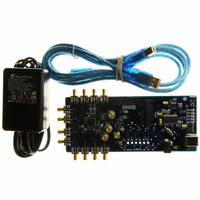
BOARD EVALUATION FOR AD9516-1
Manufacturer
Analog Devices Inc
Specifications of AD9516-1/PCBZ
Main Purpose
Timing, Clock Generator
Embedded
No
Utilized Ic / Part
AD9516-1
Primary Attributes
2 Inputs, 14 Outputs, 2.5GHz VCO
Secondary Attributes
CMOS, LVDS, LVPECL Output Logic, ADIsimCLK™ Graphical User Interface
Silicon Manufacturer
Analog Devices
Application Sub Type
PLL Clock Synthesizer
Kit Application Type
Clock & Timing
Silicon Core Number
AD9516-0, AD9516-1, AD9516-2
Silicon Family Name
AD9516-X
Rohs Compliant
Yes
Lead Free Status / RoHS Status
Lead free / RoHS Compliant


UG-075
AD9516 PLL LOOP FILTER
The AD9516 PLL requires an external loop filter whose compo-
nents are tailored for different applications. The third-order
passive configuration shown in Figure 27 usually offers the best
performance and is the one found on the evaluation board.
The default loop filter on the AD9516 evaluation board is
optimized for clock generation where the input reference is
relatively quiet. It has a transfer function with slight peaking
(<3 dB) and loop bandwidths from 75 kHz to 200 kHz. In
most of these applications, the phase detector is run at 10 MHz
to 50 MHz. Table 2 shows the correspondence between the
component numbers shown in Figure 27 and those on the
evaluation board, as well as the default values for each version
of the evaluation board. The Quick Start Guide to the AD9516
PLL section uses these default values. The phase detector
frequency is 10 MHz, and the charge pump current for this
example is 3.0 mA. The resulting loop bandwidth is 75 kHz
with 50 degrees of phase margin.
Table 2. AD9516 Default Loop Filter Values and PLL Setup
ADISimCLK Naming
C1
R1
C2
R2
C3
Input Frequency
R Divider
PFD
N Divider
VCO Frequency
ICP
AD9516
CHARGE
PUMP
VCO
Figure 27. PLL Loop Filter
Evaluation Board Location
C25
R5
C22
R2
C31
N/A
N/A
N/A
N/A
N/A
N/A
LF
CP
BYPASS
C
BP
= 220nF
C1
R1
C2
R2
C3
AD9516-0/AD9516-2/AD9516-4
470 pF
910 Ω
8.2 nF
2.4 kΩ
150 pF
1
10 MHz
−0: 280
−2: 220
−4: 160
−0: 2800 MHz
−2: 2200 MHz
−4: 1600 MHz
3.0 mA
10 MHz
Rev. 0 | Page 14 of 16
When using this loop filter, the same PLL loop dynamics
can be maintained with a higher input reference frequency
by proportionately reducing the charge pump current, or by
increasing the R divider such that the PFD frequency remains
the same.
For SONET and Ethernet line cards, as well as applications
where the reference clock is relatively high jitter, the low loop
BW loop filter shown in Table 3 is a better choice. It has a flat
transfer function with peaking <0.1 dB and loop bandwidths
from 0.5 kHz to 10 kHz. In most of these applications, the phase
detector should be run at 1 MHz or less. A loop filter design
such as this optimal for hitless reference clock switching.
The user should not consider the previous recommendations as
a substitute for using ADIsimCLK™ to determine the best loop
filter for a given application. ADIsimCLK is a free program that
can help with the design and exploration of the capabilities and
features of the AD9516, including the design of the PLL loop
filter. The website has three sample ADIsimCLK files that include
the AD9516/AD9517/AD9518 default loop filter titled:
AD9516EvalBoardExample_200MHz.clk
AD9517EvalBoardExample_200MHz.clk
AD9518EvalBoardExample_200MHz.clk
ADIsimCLK includes support for the AD9516. The AD9516,
AD9517, and AD9518 share the same loop dynamics.
ADIsimCLK is available at www.analog.com/clocks.
Evaluation Board User Guide
AD9516-1
470 pF
820 Ω
8.2 nF
2.4 kΩ
150 pF
10 MHz
1
10 MHz
250
2500 MHz
3.0 mA
AD9516-3
560 pF
750 Ω
10 nF
2 kΩ
180 pF
10 MHz
1
10 MHz
200
2000 MHz
3.0 mA
Related parts for AD9516-1/PCBZ
Image
Part Number
Description
Manufacturer
Datasheet
Request
R

Part Number:
Description:
IC CLOCK PLL/VCO 2GHZ 64LFCSP
Manufacturer:
Analog Devices Inc
Datasheet:
Part Number:
Description:
IC CLOCK GEN 2.8GHZ VCO 64-LFCSP
Manufacturer:
Analog Devices Inc
Datasheet:
Part Number:
Description:
IC,Fourteen Distributed-Output Clock Driver,LLCC,64PIN,PLASTIC
Manufacturer:
Analog Devices Inc
Datasheet:
Part Number:
Description:
IC,Ten Distributed-Output Clock Driver,LLCC,64PIN,PLASTIC
Manufacturer:
Analog Devices Inc
Datasheet:
Part Number:
Description:
IC,Ten Distributed-Output Clock Driver,LLCC,64PIN,PLASTIC
Manufacturer:
Analog Devices Inc
Datasheet:
Part Number:
Description:
Clock IC With 1.8GHz On-chip VCO
Manufacturer:
Analog Devices Inc
Datasheet:

Part Number:
Description:
BOARD EVAL FOR AD9516-3 2.0GHZ
Manufacturer:
Analog Devices Inc
Datasheet:

Part Number:
Description:
BOARD EVAL FOR AD9516-4 1.8GHZ
Manufacturer:
Analog Devices Inc
Datasheet:
Part Number:
Description:
IC,Ten Distributed-Output Clock Driver,LLCC,64PIN,PLASTIC
Manufacturer:
Analog Devices Inc
Datasheet:
Part Number:
Description:
IC,Fourteen Distributed-Output Clock Driver,LLCC,64PIN,PLASTIC
Manufacturer:
Analog Devices Inc
Datasheet:
Part Number:
Description:
IC,Ten Distributed-Output Clock Driver,LLCC,64PIN,PLASTIC
Manufacturer:
Analog Devices Inc
Datasheet:
Part Number:
Description:
Clock IC With 1.8GHz On-chip VCO
Manufacturer:
Analog Devices Inc
Datasheet:
Part Number:
Description:
10/14 Chan Clock IC W/PLL-no VCO
Manufacturer:
Analog Devices Inc
Datasheet:
Part Number:
Description:
10/14 Chan Clock IC W/PLL-no VCO
Manufacturer:
Analog Devices Inc
Datasheet:

Part Number:
Description:
Clock IC With 2.5GHz On-chip VCO EB
Manufacturer:
Analog Devices Inc
Datasheet: