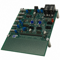
W682510DK Nuvoton Technology Corporation of America, W682510DK Datasheet - Page 12

W682510DK
Manufacturer Part Number
W682510DK
Description
KIT DEVELOPMENT FOR W682510
Manufacturer
Nuvoton Technology Corporation of America
Specifications of W682510DK
Main Purpose
Telecom, CODEC
Embedded
No
Utilized Ic / Part
W682510
Primary Attributes
Dual Voice Band PCM CODEC
Secondary Attributes
Parallel & Serial Modes, 2 RJ9 Handset Jacks
Lead Free Status / RoHS Status
Contains lead / RoHS non-compliant
This pin carries the signal ground voltage level and requires a bypass capacitor. A 0.1μF ceramic
(with low ESR for good high frequency response) capacitor needs to be connected between the V
pin and the V
Power up input signal. When the PUI pin is set to logic “0” level, the CODEC will go into power down
mode.
The PCM interface is controlled by pins PCMMS, BCLK, FSR & FST. The input data is received
through the PCMR pin and the output data is transmitted through the PCMT pin. The modes of
operation of the interface are shown in Table 7.2.
This pin selects the desired companding law. The CODEC will operate in the μ-law when this pin is at
a logic “0” level and in the A-law when at a logic “1” level. The CODEC operates μ-law if the pin is left
open, since this pin is internally pulled down.
PCMMS
7.4. PCM I
[HIGH]
[LOW]
V
V
7.3.4. V
7.3.5. PUI
7.4.1. μ/A-Law
DD
SS
REF
NTERFACE
REF
pin.
PCM Mode
Parallel
Mode
Serial Mode
TABLE 7.25: PIN-SELECTABLE COMPRESSION FORMAT
LOW (V
TABLE 7.2: PCM INTERFACE MODE SELECTIONS
μ/A-Law pin
HIGH (V
Data Available
CH1 data on PCMT1 & PCMR1
CH2 data on PCMT2 and PCMR2 (same timing as CH1)
CH1 data followed by CH2 receive data on PCMR2 (total 16 bits)
CH1 data followed by CH2 transmit data on PCMT1 (total 16 bits)
SS
), Floating
DD
)
- 12 -
Format
A-Law
μ -Law
W682510/W682310
SSA


