STEVAL-IFP007V1 STMicroelectronics, STEVAL-IFP007V1 Datasheet - Page 12
STEVAL-IFP007V1
Manufacturer Part Number
STEVAL-IFP007V1
Description
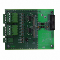
BOARD EVAL BASED ON SCLT3-8
Manufacturer
STMicroelectronics
Specifications of STEVAL-IFP007V1
Main Purpose
Interface, Digital Signal Termination
Embedded
No
Utilized Ic / Part
SCLT3-8
Primary Attributes
8 Channel Optical Isolation
Secondary Attributes
SPI Interface
Processor To Be Evaluated
SCLT3
Data Bus Width
16 bit
Interface Type
SPI
Operating Supply Voltage
24 V
Lead Free Status / RoHS Status
Lead free / RoHS Compliant
Other names
497-9045


Functional description
2.6.3
12/33
SPI transfer speed
The speed of the SPI is defined by the clock frequency and the data frame transfer time. In
the SCLT application the transfer time correspond to the input scanning time programmed
by the I/O controller.
In a 16-bit mode this scanning time should be less than 500 µs for a 64-input module (128
bits to transfer) where it should be about 160 µs for a 16-input module (32 bits to transfer).
To obtain such scanning with the data frame structure, the clock frequency is set
respectively at 256 kHz and 200 kHz.
Figure 9.
The clock frequency is limited by the application requirements to secure the immunity of the
SPI section against fast transient disturbances and keep the isolator consumption low
enough.
The SCLT maximum SPI clock frequency is 2 MHz.
●
●
In between two transfer sequences the output driver of the SPI circuit should go in high
impedance before any new transfer operation so falling edge of the chip select /CS:
t
DIS
MOSI
MISO
SCK
/CS
< t
The minimum SPI clock period is also defined by the capability of the SCLT to capture
data on MOSI and to write out data on MISO as shown in
–
–
At the start of the transfer sequence the first rising edge of the clock SCK should occur
after the data writing on the SPI output MISO corresponding with the propagation time
t
A
, avoiding missing the first data: t
DT
Capture rule: t
Write out rule: t
.
T
A
SCLT slave unit operation, input MOSI and output MISO timing diagrams
T
LD
MSB
MSB
M
S
CH
D
T
1
CH
+ t
> t
S
H
T
Doc ID 15191 Rev 3
D
< t
T
CL
T
CL
S
= t
T
14
14
2
H
C
LD
- t
> t
CH
A
+ t
S
15
1
1
T
FO
T
T
F
Table
RO
T
LSB
LSB
R
16
M
S
9.
T
HC
MSB
MSB
SCLT3-8BT8
M
S
T
DT
Related parts for STEVAL-IFP007V1
Image
Part Number
Description
Manufacturer
Datasheet
Request
R

Part Number:
Description:
BOARD EVAL SPZB260 MOD FOR STR9
Manufacturer:
STMicroelectronics
Datasheet:

Part Number:
Description:
BOARD EVAL EXTENSION SN250
Manufacturer:
STMicroelectronics
Datasheet:

Part Number:
Description:
BOARD EVAL AB-54003L-512
Manufacturer:
STMicroelectronics
Datasheet:

Part Number:
Description:
BOARD REF DESIGN RF DMOS PWR AMP
Manufacturer:
STMicroelectronics
Datasheet:

Part Number:
Description:
BOARD EVAL PWR AMP AB-84008L-470
Manufacturer:
STMicroelectronics
Datasheet:

Part Number:
Description:
BOARD EVAL FOR STM32F103XX
Manufacturer:
STMicroelectronics
Datasheet:

Part Number:
Description:
BOARD EVAL AB-54003L-512
Manufacturer:
STMicroelectronics
Datasheet:

Part Number:
Description:
BOARD SMART PLUG STM32 SPZB260PR
Manufacturer:
STMicroelectronics
Datasheet:

Part Number:
Description:
BOARD DEMO BLUETOOTH SPBT2532C2
Manufacturer:
STMicroelectronics
Datasheet:
Part Number:
Description:
ZIGBEE USB DONGLE EVAL KIT
Manufacturer:
STMicroelectronics
Datasheet:
Part Number:
Description:
STMicroelectronics [RIPPLE-CARRY BINARY COUNTER/DIVIDERS]
Manufacturer:
STMicroelectronics
Datasheet:
Part Number:
Description:
STMicroelectronics [LIQUID-CRYSTAL DISPLAY DRIVERS]
Manufacturer:
STMicroelectronics
Datasheet:

Part Number:
Description:
BOARD EVAL FOR MEMS SENSORS
Manufacturer:
STMicroelectronics
Datasheet: