CPC5621-EVAL-RDL Clare, CPC5621-EVAL-RDL Datasheet - Page 12
CPC5621-EVAL-RDL
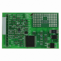
Manufacturer Part Number
CPC5621-EVAL-RDL
Description
LITELINK III EVALUATION BOARD
Manufacturer
Clare
Series
LITELINK® IIIr
Specifications of CPC5621-EVAL-RDL
Main Purpose
Telecom, Isolation Solution
Embedded
No
Utilized Ic / Part
CPC5621
Primary Attributes
Full-Wave Ringing Detection Phone Line Interface
Secondary Attributes
Resistive AC Termination
Lead Free Status / RoHS Status
Lead free / RoHS Compliant
Other names
CLA164
CPC5621EVAL-RDL
CPC5621EVAL-RDL


CPC5620/CPC5621
signal and coupled across the electrical isolation
barrier by a reflective dome.
On the equipment’s low voltage side of the barrier, the
receive signal is converted by a photodiode into a
photocurrent. The photocurrent, a linear
representation of the receive signal, is amplified and
converted to a differential voltage output on RX+ and
RX-.
Variations in gain are controlled to within ±0.4 dB by
factory gain trim, which sets the output to unity gain.
To accommodate single-supply operation, LITELINK
includes a small DC bias on the RX outputs of 1.0V
Most applications should AC couple the RX outputs as
shown in Figure 5.
LITELINK may be used for differential or single-ended
output as shown in Figure 5. Single-ended use will
produce 6 dB less signal output amplitude. Do not
exceed 0 dBm into 600 Ω (2.2 V
the standard application circuit. See application note
AN-157,
information.
Figure 5. Differential and Single-ended Receive
3.3.2 Transmit Signal Path
Connect transmit signals from the low-voltage side
equipment to the TX+ and TX- pins of LITELINK. Do
not exceed a signal level of 0 dBm in 600 Ω (or 2.2
V
single-ended signals in LITELINK. The signal is
coupled to the transmit photodiode amplifier in a
similar manner to the receive path. See application
note AN-157,
more information.
12
P-P
). Differential transmit signals are converted to
Low-Voltage Side CODEC
or Voice Circuit
Increased LITELINK III Transmit Power
Path Connections to LITELINK
RX+
RX-
RX
Increased LITELINK III Transmit Power
0.1µF
0.1µF
0.1µF
P-P
LITELINK
RX+
RX-
RX+
) signal input with
for more
for
www.clare.com
DC
.
The output of the photodiode amplifier is coupled to a
voltage-to-current converter via a transconductance
stage where the transmit signal modulates the
telephone line loop current. As in the receive path,
gain is set to unity at the factory, limiting insertion loss
variation to ±0.4 dB.
Differential and single-ended transmit signals into
LITELINK should not exceed a signal level of 0 dBm
referenced to 600 Ω (or 2.2 V
levels above 0dBm consult the application note
AN-157,
information.
Figure 6. Differential and Single-ended Transmit
3.4 Start-up Requirements
OH must be de-asserted (set logic high) once after
power-up for at least 50ms to transfer internal gain
trim values within LITELINK. This would be normal
operation in most applications. Failure to comply with
this requirement will result in transmission gain errors
and possibly distortion.
3.5 DC Characteristics
The CPC5620 and CPC5621 are designed for
worldwide application, including use under the
requirements of TBR-21. The ZDC, DCS1, and DCS2
pins control the VI slope characteristics of LITELINK.
Selecting appropriate resistor values for R
and R
assure compliance with DC requirements.
Low-Voltage Side CODEC or
Transmit Circuit
Low-Voltage Side CODEC or
Transmit Circuit
DCS
TXA1
TXA2
TXA1
Increased LITELINK III Transmit Power
(R15) in the provided application circuits
Path Connections to LITELINK
0.1 µ f
0.1 µ f
0.1 µ f
0.1 µ f
LITELINK
LITELINK
TX+
TX-
TX-
TX+
P-P
). For output power
-
+
+
-
ZDC
for more
(R16)
R04
Related parts for CPC5621-EVAL-RDL
Image
Part Number
Description
Manufacturer
Datasheet
Request
R

Part Number:
Description:
LITELINK III EVALUATION BOARD
Manufacturer:
Clare
Datasheet:

Part Number:
Description:
Clare Solar Cells
Manufacturer:
Clare, Inc.
Datasheet:
Part Number:
Description:
Clare Solar Cells
Manufacturer:
Clare, Inc.
Datasheet:
Part Number:
Description:
4 Pin SOP OptoMOS Relay
Manufacturer:
CLARE [Clare, Inc.]
Datasheet:

Part Number:
Description:
MOSFET N-CH 350V 5MA SOT-223
Manufacturer:
Clare
Datasheet:
Part Number:
Description:
MOSFET N-CH 350V 5MA SOT-223
Manufacturer:
Clare
Datasheet:

Part Number:
Description:
IC DRVR PROGRAMMABLE 16-SOIC
Manufacturer:
Clare
Datasheet:

Part Number:
Description:
IC PHONE LINE MONITOR 8-SOIC
Manufacturer:
Clare
Datasheet:

Part Number:
Description:
IC LITELINK III FULL RING 32SOIC
Manufacturer:
Clare
Datasheet:

Part Number:
Description:
LITELINK III PHONE LINE 32SOIC
Manufacturer:
Clare
Datasheet:

Part Number:
Description:
RELAY OPTO TELCOM 12OMA 8-DIP
Manufacturer:
Clare
Datasheet: