ATA6625-EK Atmel, ATA6625-EK Datasheet - Page 3
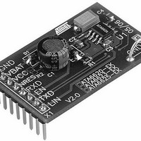
ATA6625-EK
Manufacturer Part Number
ATA6625-EK
Description
BOARD DEMO LIN SBC FOR ATA6625
Manufacturer
Atmel
Specifications of ATA6625-EK
Main Purpose
Interface, LIN
Embedded
Yes, MCU, 8-Bit
Utilized Ic / Part
ATA6625
Primary Attributes
LIN-SBC (System-Basis-Chip) Transceiver, LIN 2.0, Voltage Regulator
Secondary Attributes
4 Power Modes: Pre-Normal, Normal, Sleep, Silent, 8-SOIC
Lead Free Status / RoHS Status
Contains lead / RoHS non-compliant


3. Functional Description
3.1
3.2
3.3
3.4
3.5
3.6
4957I–AUTO–03/11
Physical Layer Compatibility
Supply Pin (VS)
Ground Pin (GND)
Voltage Regulator Output Pin (VCC)
Undervoltage Reset Output (NRES)
Bus Pin (LIN)
Since the LIN physical layer is independent from higher LIN layers (e.g., LIN protocol layer), all
nodes with a LIN physical layer according to revision 2.x can be mixed with LIN physical layer
nodes, which are according to older versions (i.e., LIN 1.0, LIN 1.1, LIN 1.2, LIN 1.3) without
any restrictions.
LIN operating voltage is V
transmission if V
the IC starts with the Fail-safe Mode and the voltage regulator is switched on.
The supply current in Sleep Mode is typically 10µA and 57µA in Silent Mode.
The IC does not affect the LIN Bus in the event of GND disconnection. It is able to handle a
ground shift up to 11.5% of V
The internal 3.3V/5V voltage regulator is capable of driving loads up to 85mA, supplying the
microcontroller and other ICs on the PCB and is protected against overload by means of cur-
rent limitation and overtemperature shut-down. Furthermore, the output voltage is monitored
and will cause a reset signal at the NRES output pin if it drops below a defined threshold V
If the V
low after tres_f
internally driven from the V
V
The implemented undervoltage delay keeps NRES low for t
nominal value.
A low-side driver with internal current limitation and thermal shutdown as well as an internal
pull-up resistor according to LIN specification 2.x is implemented. The voltage range is from
–27V to +40V. This pin exhibits no reverse current from the LIN bus to V
a GND shift or V
protocol specification.
The fall time (from recessive to dominant) and the rise time (from dominant to recessive) are
slope controlled.
S
< 1.5V and then becomes highly resistant.
CC
voltage falls below the undervoltage detection threshold of V
(Figure 6-1 on page
S
Batt
falls below 5V, in order to avoid false bus messages. After switching on V
disconnection. The LIN receiver thresholds are compatible with the LIN
S
= 5V to 27V. An undervoltage detection is implemented to disable
S
S
.
voltage. If V
11). Even if V
S
Atmel ATA6623/ATA6625
voltage ramps down, NRES stays low until
CC
= 0V the NRES stays low, because it is
Reset
= 4ms after V
thun
S
, even in the event of
, NRES switches to
CC
reaches its
thun
S
3
,
.
Related parts for ATA6625-EK
Image
Part Number
Description
Manufacturer
Datasheet
Request
R

Part Number:
Description:
Lin Bus Transceiver With Integrated Vol Tage Regulator
Manufacturer:
ATMEL Corporation
Datasheet:
Part Number:
Description:
(ATA6623 / ATA6625) LIN Bus Transceiver
Manufacturer:
ATMEL Corporation
Datasheet:

Part Number:
Description:
LIN Bus Transceiver with Integrated Voltage Regulator
Manufacturer:
ATMEL [ATMEL Corporation]
Datasheet:

Part Number:
Description:
TXRX LIN BUS 5V W/VREG 8SOIC
Manufacturer:
Atmel
Datasheet:
Part Number:
Description:
TXRX LIN BUS 5V W/VREG 8SOIC
Manufacturer:
Atmel
Datasheet:


Part Number:
Description:
DEV KIT FOR AVR/AVR32
Manufacturer:
Atmel
Datasheet:
Part Number:
Description:
INTERVAL AND WIPE/WASH WIPER CONTROL IC WITH DELAY
Manufacturer:
ATMEL Corporation
Datasheet:
Part Number:
Description:
Low-Voltage Voice-Switched IC for Hands-Free Operation
Manufacturer:
ATMEL Corporation
Datasheet:
Part Number:
Description:
MONOLITHIC INTEGRATED FEATUREPHONE CIRCUIT
Manufacturer:
ATMEL Corporation
Datasheet:
Part Number:
Description:
AM-FM Receiver IC U4255BM-M
Manufacturer:
ATMEL Corporation
Datasheet:
Part Number:
Description:
Monolithic Integrated Feature Phone Circuit
Manufacturer:
ATMEL Corporation
Datasheet:
Part Number:
Description:
Multistandard Video-IF and Quasi Parallel Sound Processing
Manufacturer:
ATMEL Corporation
Datasheet: