ATA6625-EK Atmel, ATA6625-EK Datasheet - Page 6
ATA6625-EK
Manufacturer Part Number
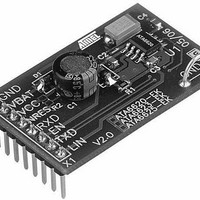
ATA6625-EK
Description
BOARD DEMO LIN SBC FOR ATA6625
Manufacturer
Atmel
Specifications of ATA6625-EK
Main Purpose
Interface, LIN
Embedded
Yes, MCU, 8-Bit
Utilized Ic / Part
ATA6625
Primary Attributes
LIN-SBC (System-Basis-Chip) Transceiver, LIN 2.0, Voltage Regulator
Secondary Attributes
4 Power Modes: Pre-Normal, Normal, Sleep, Silent, 8-SOIC
Lead Free Status / RoHS Status
Contains lead / RoHS non-compliant


4.1
4.2
6
Normal Mode
Silent Mode
Atmel ATA6623/ATA6625
This is the normal transmitting and receiving Mode of the LIN Interface, in accordance with LIN
specification 2.x. The V
tolerance of ±2% and a maximum output current of 85mA.
If an undervoltage condition occurs, NRES is switched to low and the IC changes its state to
Fail-safe Mode.
A falling edge at EN while TXD is high switches the IC into Silent Mode. The TXD Signal has
to be logic high during the Mode Select window
is disabled in Silent Mode. The overall supply current from V
I
In Silent Mode the internal slave termination between pin LIN and pin VS is disabled, and only
a weak pull-up current (typically 10µA) between pin LIN and pin VS is present. The Silent
Mode can be activated independently from the current level on pin LIN.
If an undervoltage condition occurs, NRES is switched to low and the IC changes its state to
Fail-safe Mode.
A voltage less than the LIN Pre-wake detection V
receiver and switches on the internal slave termination between the LIN pin and the VS pin.
A falling edge at the LIN pin followed by a dominant bus level maintained for a certain time
period (> t
remote wake-up request.
The device switches from Silent Mode to Fail-safe Mode, and the remote wake-up request is
indicated by a low level at pin RXD to interrupt the microcontroller
high can be used to switch directly to Normal Mode.
VSsi
= 57µA plus the V
bus
) and the following rising edge at pin LIN (see
CC
CC
regulator output current I
voltage regulator operates with a 3.3V/5V output voltage, with a low
(Figure 4-2 on page
VCC
LINL
.
at pin LIN activates the internal LIN
Figure 4-3 on page
Batt
(Figure 4-3 on page
7). The transmission path
is a combination of the
4957I–AUTO–03/11
7) results in a
7). EN
Related parts for ATA6625-EK
Image
Part Number
Description
Manufacturer
Datasheet
Request
R

Part Number:
Description:
Lin Bus Transceiver With Integrated Vol Tage Regulator
Manufacturer:
ATMEL Corporation
Datasheet:
Part Number:
Description:
(ATA6623 / ATA6625) LIN Bus Transceiver
Manufacturer:
ATMEL Corporation
Datasheet:

Part Number:
Description:
LIN Bus Transceiver with Integrated Voltage Regulator
Manufacturer:
ATMEL [ATMEL Corporation]
Datasheet:

Part Number:
Description:
TXRX LIN BUS 5V W/VREG 8SOIC
Manufacturer:
Atmel
Datasheet:
Part Number:
Description:
TXRX LIN BUS 5V W/VREG 8SOIC
Manufacturer:
Atmel
Datasheet:


Part Number:
Description:
DEV KIT FOR AVR/AVR32
Manufacturer:
Atmel
Datasheet:
Part Number:
Description:
INTERVAL AND WIPE/WASH WIPER CONTROL IC WITH DELAY
Manufacturer:
ATMEL Corporation
Datasheet:
Part Number:
Description:
Low-Voltage Voice-Switched IC for Hands-Free Operation
Manufacturer:
ATMEL Corporation
Datasheet:
Part Number:
Description:
MONOLITHIC INTEGRATED FEATUREPHONE CIRCUIT
Manufacturer:
ATMEL Corporation
Datasheet:
Part Number:
Description:
AM-FM Receiver IC U4255BM-M
Manufacturer:
ATMEL Corporation
Datasheet:
Part Number:
Description:
Monolithic Integrated Feature Phone Circuit
Manufacturer:
ATMEL Corporation
Datasheet:
Part Number:
Description:
Multistandard Video-IF and Quasi Parallel Sound Processing
Manufacturer:
ATMEL Corporation
Datasheet: