ATA6826-DK Atmel, ATA6826-DK Datasheet - Page 4
ATA6826-DK
Manufacturer Part Number
ATA6826-DK
Description
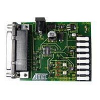
BOARD EVALUATION FOR ATA6826
Manufacturer
Atmel
Specifications of ATA6826-DK
Main Purpose
Power Management, Half H-Bridge Driver (Internal FET)
Embedded
No
Utilized Ic / Part
ATA6826
Primary Attributes
3 Half H-Bridge Drivers, 1A, 2 kV ESD Protection
Secondary Attributes
Short-Circuit, Thermal & Undervoltage Protection
Lead Free Status / RoHS Status
Contains lead / RoHS non-compliant


3. Functional Description
3.1
Figure 3-1.
4
CLK
DO
CS
DI
Serial Interface
Atmel ATA6826
Data Transfer
0
SRR
TP
1
S1L
LS1
Data transfer starts with the falling edge of the CS signal. Data must appear at DI synchronized
to CLK and is accepted on the falling edge of the CLK signal. LSB (bit 0, SRR) has to be
transferred first. Execution of new input data is enabled on the rising edge of the CS signal.
When CS is high, pin DO is in tri-state condition. This output is enabled on the falling edge of
CS. Output data will change their state with the rising edge of CLK and stay stable until the next
rising edge of CLK appears. LSB (bit 0, TP) is transferred first.
Table 3-1.
2
S1H
HS1
Bit
10
11
12
13
14
15
0
1
2
3
4
5
6
7
8
9
3
S2L
LS2
Input Register
4
Input Data Protocol
S2H
HS2
OCS
SRR
HS1
HS2
HS3
n. u.
n. u.
n. u.
n. u.
n. u.
n. u.
n. u.
n. u.
LS1
LS2
LS3
5
S3L
LS3
6
S3H
HS3
Function
Status register reset (high = reset; the bits PSF, OPL and SCD in the
output data register are set to low)
Controls output LS1 (high = switch output LS1 on)
Controls output HS1 (high = switch output HS1 on)
See LS1
See HS1
See LS1
See HS1
Not used
Not used
Not used
Not used
Not used
Not used
Overcurrent shutdown (high = overcurrent shutdown is active)
Not used
Not used
7
n. u.
n. u.
8
n. u.
n. u.
9
n. u.
n. u.
10
n. u.
n. u.
11
n. u.
n. u.
12
n. u.
n. u.
13
SCD
OCS
14
OPL
n. u.
15
4834G–BCD–01/11
PSF
n. u.
Related parts for ATA6826-DK
Image
Part Number
Description
Manufacturer
Datasheet
Request
R

Part Number:
Description:
Triple Half-bridge DMOS Output Driver with Serial Input Control
Manufacturer:
ATMEL Corporation
Datasheet:

Part Number:
Description:
MOSFET & Power Driver ICs Triple Half-Bridge Driver
Manufacturer:
Atmel
Datasheet:
Part Number:
Description:
MOSFET & Power Driver ICs Triple Half-Bridge Driver
Manufacturer:
Atmel
Datasheet:

Part Number:
Description:
DEV KIT FOR AVR/AVR32
Manufacturer:
Atmel
Datasheet:
Part Number:
Description:
INTERVAL AND WIPE/WASH WIPER CONTROL IC WITH DELAY
Manufacturer:
ATMEL Corporation
Datasheet:
Part Number:
Description:
Low-Voltage Voice-Switched IC for Hands-Free Operation
Manufacturer:
ATMEL Corporation
Datasheet:
Part Number:
Description:
MONOLITHIC INTEGRATED FEATUREPHONE CIRCUIT
Manufacturer:
ATMEL Corporation
Datasheet:
Part Number:
Description:
AM-FM Receiver IC U4255BM-M
Manufacturer:
ATMEL Corporation
Datasheet:
Part Number:
Description:
Monolithic Integrated Feature Phone Circuit
Manufacturer:
ATMEL Corporation
Datasheet:
Part Number:
Description:
Multistandard Video-IF and Quasi Parallel Sound Processing
Manufacturer:
ATMEL Corporation
Datasheet:
Part Number:
Description:
High-performance EE PLD
Manufacturer:
ATMEL Corporation
Datasheet:
Part Number:
Description:
8-bit Flash Microcontroller
Manufacturer:
ATMEL Corporation
Datasheet: