RDK-128 Power Integrations, RDK-128 Datasheet - Page 3
RDK-128
Manufacturer Part Number
RDK-128
Description
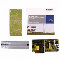
KIT REF DESIGN 36-72W MOTOR DRVR
Manufacturer
Power Integrations
Specifications of RDK-128
Main Purpose
Power Management, Motor Control
Embedded
No
Utilized Ic / Part
PKS606
Primary Attributes
Variable Speed 12V 36W DC Motor, 90 ~ 265 VAC
Secondary Attributes
External Potentiometer or Variable DC Voltage Speed Control
Lead Free Status / RoHS Status
Not applicable / Not applicable
Other names
596-1198


PeakSwitch Functional Description
PeakSwitch integrates a 700 V power MOSFET switch with a
power supply controller on the same die. Unlike conventional
pulse width modulation (PWM) controllers, PeakSwitch uses a
simple ON/OFF control to regulate the output voltage.
The controller consists of an oscillator, enable
circuit (sense and logic), current-limit state machine,
5.8 V regulator, BYPASS pin under-voltage circuit, over-
temperature protection, current limit circuit, and leading
edge blanking. PeakSwitch incorporates additional circuitry
for adaptive current limit, line under-voltage sense,
programmable smart line sense, auto-restart, adaptive
switching cycle on-time extension, and frequency jitter.
Figure 2 is a functional block diagram of the device’s most
important features.
Oscillator
The typical oscillator frequency is internally set to an average
of 277 kHz. Two signals are generated from the oscillator: the
maximum duty cycle (DC
indicates the beginning of each cycle.
The oscillator incorporates circuitry that introduces a small
amount of frequency jitter, typically 16 kHz peak-to-peak, to
minimize EMI emission. The modulation rate of the frequency
jitter is set to 1.1 kHz to optimize EMI reduction for both
average and quasi-peak emissions. The frequency jitter should
be measured with the oscilloscope triggered at the falling edge
of the DRAIN waveform. The waveform in Figure 4 illustrates
the frequency jitter.
Enable Input and Current-Limit State Machine
The enable input circuit at the EN/UV pin consists of a low
impedance source follower output set at 1.0 V. The current
600
500
400
300
200
100
Figure 4. Frequency Jitter.
0
0
MAX
Time (µs)
285 kHz
269 kHz
V
) signal and the clock signal that
DRAIN
2.5
5
through the source follower is limited to 240 µA. When the
current out of this pin exceeds 240 µA, a low logic level
(disable) is generated at the output of the enable circuit. This
enable circuit output is sampled at the beginning of each
cycle on the rising edge of the clock signal. If high, the power
MOSFET is turned on for that cycle (enabled). If low, the power
MOSFET remains off (disabled). Since the sampling is done
only at the beginning of each cycle, subsequent changes in the
EN/UV pin voltage or current during the remainder of the
cycle are ignored.
The current-limit state machine reduces the current limit by
discrete amounts at light loads when PeakSwitch is likely to
switch in the audible frequency range. The lower current limit
raises the effective switching frequency above the audio range
and reduces the transformer flux density, including the associated
audible noise. The state machine monitors the sequence of
EN/UV pin voltage levels to determine the load condition and
adjusts the current limit level accordingly in discrete amounts.
Under most operating conditions (except when close to no-load),
the low impedance of the source follower keeps the voltage on
the EN/UV pin from going much below 1.0 V in the disabled
state. This improves the response time of the optocoupler that
is usually connected to this pin.
5.8 V Regulator and 6.3 V Shunt Voltage Clamp
The 5.8 V regulator charges the bypass capacitor connected to
the BYPASS pin to 5.8 V by drawing a current from the voltage
on the DRAIN pin whenever the MOSFET is off. The BYPASS
pin is the internal supply voltage node. When the MOSFET
is on, the PeakSwitch operates from the energy stored in the
bypass capacitor. The voltage on the DRAIN pin powers the
bypass during start-up.
There is a 6.3 V shunt regulator clamping the BYPASS pin at
6.3 V when current is provided through an external resistor
from the bias winding in normal operation. Powering the
PeakSwitch device in this way minimizes no-load consumption
to about 150 mW at 265 VAC. Note that a bias winding must be
used to power the device. See Key Application Considerations
section for details.
BYPASS Pin Under-Voltage
The BYPASS pin under-voltage circuitry disables the power
MOSFET when the BYPASS pin voltage drops below 4.8 V.
Once the BYPASS pin voltage drops below 4.8 V, it must rise
back to 5.8 V to enable (turn on) the power MOSFET.
Over Temperature Protection
The thermal shutdown circuitry senses the die temperature.
The threshold is typically set at 142 °C with 75 °C hysteresis.
When the die temperature rises above this threshold, the
power MOSFET is disabled and remains disabled until the die
temperature falls by 75 °C, at which point it is re-enabled. A large
PKS603-607
Rev. I 02/07
3
Related parts for RDK-128
Image
Part Number
Description
Manufacturer
Datasheet
Request
R

Part Number:
Description:
KIT REF DESIGN FOR LNK457D
Manufacturer:
Power Integrations
Datasheet:

Part Number:
Description:
REFERENCE DESIGN LINKSWITCH-PH
Manufacturer:
Power Integrations
Datasheet:

Part Number:
Description:
KIT REF DESIGN FOR LNK403EG
Manufacturer:
Power Integrations
Datasheet:

Part Number:
Description:
KIT REF DESIGN FOR LNK406EG
Manufacturer:
Power Integrations
Datasheet:

Part Number:
Description:
KIT REF DESIGN LINKSWITCH-CV
Manufacturer:
Power Integrations
Datasheet:

Part Number:
Description:
KIT REF DESIGN LINKSWITCH 2
Manufacturer:
Power Integrations
Datasheet:

Part Number:
Description:
Specifications: Family: Eval Boards - DC/DC & AC/DC (Off-Line) SMPS ; Series: HiperLCS™ ; Main Purpose: DC/DC, Step Down ; Outputs and Type: 1, Isolated ; Power - Output: 150W ; Voltage - Output: 24V ; Current - Output: 6.25A ; Voltage - Input:
Manufacturer:
Power Integrations, Inc.
Datasheet:

Part Number:
Description:
KIT DESIGN REF TINYSWITCH-III
Manufacturer:
Power Integrations
Datasheet:

Part Number:
Description:
KIT DESIGN REF LINKSWITCH LP
Manufacturer:
Power Integrations
Datasheet:

Part Number:
Description:
KIT REF DESIGN LED LINKSWITCH TN
Manufacturer:
Power Integrations
Datasheet:
Part Number:
Description:
KIT REF DESIGN FOR LNK457D
Manufacturer:
Power Integrations
Datasheet:
Part Number:
Description:
REFERENCE DESIGN LINKSWITCH-PH
Manufacturer:
Power Integrations
Datasheet:
Part Number:
Description:
Specifications: Manufacturer: Power Integrations ; Output Voltage: 380 VDC ; Input / Supply Voltage (Max): 264 VAC ; Input / Supply Voltage (Min): 90 VAC ; Mounting Style: Through Hole ; Output Current: 0.913 A ; Output Power: 347 W
Manufacturer:
Power Integrations, Inc.
Part Number:
Description:
Specifications: Family: Eval Boards - DC/DC & AC/DC (Off-Line) SMPS ; Series: HiperLCS™ ; Main Purpose: DC/DC, Step Down ; Outputs and Type: 1, Isolated ; Power - Output: 150W ; Voltage - Output: 24V ; Current - Output: 6.25A ; Voltage - Input:
Manufacturer:
Power Integrations, Inc.
Datasheet: