RDK-131 Power Integrations, RDK-131 Datasheet
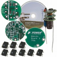
RDK-131
Specifications of RDK-131


Related parts for RDK-131


RDK-131 Summary of contents
Page 1
LNK302/304-306 LinkSwitch-TN Family Lowest Component Count, Energy-Effi cient Off-Line Switcher IC Product Highlights Cost Effective Linear/Cap Dropper Replacement • Lowest cost and component count buck converter solution • Fully integrated auto-restart for short-circuit and open loop fault protection – saves ...
Page 2
LNK302/304-306 BYPASS (BP) 6.3 V FEEDBACK 1. (FB) Figure 2a. Functional Block Diagram (LNK302). BYPASS (BP) 6.3 V FEEDBACK 1. (FB) Figure 2b. Functional Block Diagram (LNK304-306). 2-2 2 Rev. I 11/08 BYPASS PIN ...
Page 3
Pin Functional Description DRAIN (D) Pin: Power MOSFET drain connection. Provides internal operating current for both start-up and steady-state operation. BYPASS (BP) Pin: Connection point for a 0.1 μF external bypass capacitor for the internally generated 5.8 V supply. FEEDBACK ...
Page 4
LNK302/304-306 600 500 V DRAIN 400 300 200 100 0 68 kHz 64 kHz 0 Time (μs) Figure 4. Frequency Jitter. power MOSFET is turned off for the remainder of that cycle. The leading edge blanking circuit inhibits the current ...
Page 5
RF1 INPUT D4 Optimize hatched copper areas ( ) for heatsinking and EMI. Figure 6a. Recommended Printed Circuit Layout for LinkSwitch- Buck Converter Confi guration using Package. D3 RF1 AC C4 INPUT ...
Page 6
LNK302/304-306 TOPOLOGY BASIC CIRCUIT SCHEMATIC High-Side Buck – Direct FB BP Feedback LinkSwitch- High-Side Buck – Optocoupler Feedback LinkSwitch- Low-Side + Buck – Optocoupler LinkSwitch-TN Feedback V IN ...
Page 7
... The typical inductance value and RMS current rating can be obtained from the LinkSwitch-TN design spreadsheet available within the PI Expert design suite from Power Integrations. Choose L1 greater than or equal to the typical calculated inductance with RMS current rating greater than or equal to calculated RMS inductor current ...
Page 8
LNK302/304-306 Pre-load Resistor R4 In high-side, direct feedback designs where the minimum load is <3 mA, a pre-load resistor is required to maintain output regulation. This ensures suffi cient inductor energy to pull the inductor side of the feedback capacitor ...
Page 9
DRAIN Voltage .................................. ................ -0 700 V Peak DRAIN Current (LNK302).................200 mA (375 mA) Peak DRAIN Current (LNK304).................400 mA (750 mA) Peak DRAIN Current (LNK305).................800 mA (1500 mA) Peak DRAIN Current (LNK306).................1400 mA (2600 mA) FEEDBACK Voltage .........................................-0.3 ...
Page 10
LNK302/304-306 Parameter Symbol CONTROL FUNCTIONS (cont.) I CH1 BYPASS Pin Charge Current I CH2 BYPASS Pin V Voltage BP BYPASS Pin V Voltage Hysteresis BPH BYPASS Pin I Supply Current BPSC CIRCUIT PROTECTION I (See Current Limit LIMIT Note E) ...
Page 11
Parameter Symbol CIRCUIT PROTECTION (cont.) Thermal Shutdown T Hysteresis SHD OUTPUT ON-State R Resistance DS(ON) OFF-State Drain I Leakage Current DSS Breakdown Voltage BV DSS t Rise Time R t Fall Time F DRAIN Supply Voltage Output Enable t Delay ...
Page 12
LNK302/304-306 NOTES: A. Total current consumption is the sum of I switching) and the sum of I and Since the output MOSFET is switching diffi cult to isolate the switching current from the supply current ...
Page 13
Typical Performance Characteristics 1.1 1.0 0.9 -50 - 100 125 150 Junction Temperature (°C) Figure 10. Breakdown vs. Temperature. 1.4 1.2 1.0 0.8 Normalized di/dt 0.6 0.4 0 Temperature (°C) Figure 12. ...
Page 14
LNK302/304-306 Typical Performance Characteristics (cont.) PART ORDERING INFORMATION LNK 304 2-14 14 Rev. I 11/08 1000 100 Scaling Factors: LNK302 0.5 LNK304 1.0 LNK305 2.0 LNK306 3 100 200 300 400 500 Drain ...
Page 15
D S .004 (.10) -E- .240 (6.10) .260 (6.60) Pin 1 .367 (9.32) -D- .387 (9.83) .125 (3.18) .145 (3.68) -T- SEATING PLANE .100 (2.54) BSC .048 (1.22) .053 (1.35) .014 (.36) ⊕ .010 (.25) ...
Page 16
LNK302/304-306 B 4 4.90 (0.193) BSC 3.90 (0.154) BSC 0.10 (0.004 Pin 1 ID 1.27 (0.050) BSC 1.35 (0.053) 1.25 - 1.65 1.75 (0.069) (0.049 - 0.065) 0.10 (0.004) 0.25 (0.010) Reference Solder ...
Page 17
LNK302/304-306 Notes 2-17 17 Rev. I 11/08 ...
Page 18
LNK302/304-306 2-18 18 Rev. I 11/08 Notes ...
Page 19
Revision Notes C 1) Released fi nal data sheet Corrected Minimum On Time Added LNK302 Added lead-free ordering information Minor error corrections. 2) Renamed Feedback Pin Voltage parameter to Feedback Pin Voltage ...
Page 20
... The products and applications illustrated herein (including transformer construction and circuits external to the products) may be covered by one or more U.S. and foreign patents, or potentially by pending U.S. and foreign patent applications assigned to Power Integrations. A complete list of Power Integrations patents may be found at www.powerint.com. Power Integrations grants its customers a license under certain patent rights as set forth at http://www ...