RDK-131 Power Integrations, RDK-131 Datasheet - Page 5
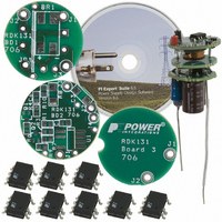
RDK-131
Manufacturer Part Number
RDK-131
Description
KIT REF DESIGN LED LINKSWITCH TN
Manufacturer
Power Integrations
Series
LinkSwitch-TNr
Specifications of RDK-131
Current - Output / Channel
300mA
Outputs And Type
1, Non-Isolated
Voltage - Output
10V
Features
fits within GU10 lamp base
Voltage - Input
85 ~ 265VAC
Utilized Ic / Part
LNK306DN
Lead Free Status / RoHS Status
Not applicable / Not applicable
Other names
596-1127


Figure 6a. Recommended Printed Circuit Layout for LinkSwitch-TN in a Buck Converter Confi guration using P or G Package.
Figure 6b. Recommended Printed Circuit Layout for LinkSwitch-TN in a Buck Converter Confi guration using D Package
cycles are skipped. To provide overload protection if no cycles
are skipped during a 50 ms period, LinkSwitch-TN will enter
auto-restart (LNK304-306), limiting the average output power
to approximately 6% of the maximum overload power. Due to
tracking errors between the output voltage and the voltage across
C3 at light load or no load, a small pre-load may be required
(R4). For the design in Figure 5, if regulation to zero load is
required, then this value should be reduced to 2.4 kΩ.
Key Application Considerations
LinkSwitch-TN Design Considerations
Output Current Table
Data sheet maximum output current table (Table 1) represents
the maximum practical continuous output current for both
mostly discontinuous conduction mode (MDCM) and continuous
conduction mode (CCM) of operation that can be delivered from
a given LinkSwitch-TN device under the following assumed
conditions:
INPUT
Optimize hatched copper areas (
AC
INPUT
AC
to Bottom Side of the Board.
RF1
RF1
D4
D4
D3
D3
C4
C4
) for heatsinking and EMI.
L2
L2
C5
Optimize hatched copper areas (
C5
FB
BP
D
S
S
D
LinkSwitch-TN
C1
1) Buck converter topology.
2) The minimum DC input voltage is ≥70 V. The value of
3) For CCM operation a KRP* of 0.4.
4) Output voltage of 12 VDC.
5) Effi ciency of 75%.
6) A catch/freewheeling diode with t
7) The part is board mounted with SOURCE pins soldered
*KRP is the ratio of ripple to peak inductor current.
LinkSwitch-TN Selection and Selection Between
MDCM and CCM Operation
Select the LinkSwitch-TN device, freewheeling diode and output
inductor that gives the lowest overall cost. In general, MDCM
input capacitance should be large enough to meet this
criterion.
MDCM operation and for CCM operation, a diode with
t
to a suffi cient area of copper to keep the SOURCE pin
temperature at or below 100 °C.
rr
S
S
S
S
≤35 ns is used.
R3
) for heatsinking and EMI.
FB
BP
S
S
D1
R1
C1
C3
R3
L1
R1
LNK302/304-306
C3
D2
D1
rr
≤75 ns is used for
PI-4546-011807
C2
L1
D2
C2
PI-3750-121106
OUTPUT
OUTPUT
DC
DC
Rev. I 11/08
2-5
5
+
+
Related parts for RDK-131
Image
Part Number
Description
Manufacturer
Datasheet
Request
R

Part Number:
Description:
KIT REF DESIGN FOR LNK457D
Manufacturer:
Power Integrations
Datasheet:

Part Number:
Description:
REFERENCE DESIGN LINKSWITCH-PH
Manufacturer:
Power Integrations
Datasheet:

Part Number:
Description:
KIT REF DESIGN FOR LNK403EG
Manufacturer:
Power Integrations
Datasheet:

Part Number:
Description:
KIT REF DESIGN FOR LNK406EG
Manufacturer:
Power Integrations
Datasheet:

Part Number:
Description:
KIT REF DESIGN LINKSWITCH-CV
Manufacturer:
Power Integrations
Datasheet:

Part Number:
Description:
KIT REF DESIGN LINKSWITCH 2
Manufacturer:
Power Integrations
Datasheet:

Part Number:
Description:
Specifications: Family: Eval Boards - DC/DC & AC/DC (Off-Line) SMPS ; Series: HiperLCS™ ; Main Purpose: DC/DC, Step Down ; Outputs and Type: 1, Isolated ; Power - Output: 150W ; Voltage - Output: 24V ; Current - Output: 6.25A ; Voltage - Input:
Manufacturer:
Power Integrations, Inc.
Datasheet:

Part Number:
Description:
KIT DESIGN REF TINYSWITCH-III
Manufacturer:
Power Integrations
Datasheet:

Part Number:
Description:
KIT DESIGN REF LINKSWITCH LP
Manufacturer:
Power Integrations
Datasheet:
Part Number:
Description:
KIT REF DESIGN PG LINKSWITCH-II
Manufacturer:
Power Integrations
Datasheet:
Part Number:
Description:
REFERENCE DESIGN LINKSWITCH-PL
Manufacturer:
Power Integrations
Datasheet:
Part Number:
Description:
REFERENCE DESIGN LINKSWITCH-PH
Manufacturer:
Power Integrations
Datasheet:

Part Number:
Description:
KIT REF DESIGN 36-72W MOTOR DRVR
Manufacturer:
Power Integrations
Datasheet:
Part Number:
Description:
Specifications: Manufacturer: Power Integrations ; Output Voltage: 380 VDC ; Input / Supply Voltage (Max): 264 VAC ; Input / Supply Voltage (Min): 90 VAC ; Mounting Style: Through Hole ; Output Current: 0.913 A ; Output Power: 347 W
Manufacturer:
Power Integrations, Inc.

Part Number:
Description:
KIT REF DESIGN TOP HX FOR TOP258
Manufacturer:
Power Integrations
Datasheet: