CDB5467U Cirrus Logic Inc, CDB5467U Datasheet - Page 31
CDB5467U
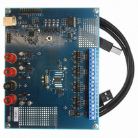
Manufacturer Part Number
CDB5467U
Description
BOARD EVAL FOR CS5467 ADC
Manufacturer
Cirrus Logic Inc
Type
A/Dr
Specifications of CDB5467U
Main Purpose
Power Management, Energy/Power Meter
Embedded
Yes, MCU, 8-Bit
Utilized Ic / Part
CS5467
Primary Attributes
Watt-Hour Meter
Secondary Attributes
Graphical User Interface, SPI™ & USB Interfaces
Product
Data Conversion Development Tools
Maximum Clock Frequency
4 MHz
Interface Type
USB
Supply Voltage (max)
5 V
Supply Voltage (min)
3.3 V
For Use With/related Products
CS5467
Lead Free Status / RoHS Status
Contains lead / RoHS non-compliant
Lead Free Status / RoHS Status
Lead free / RoHS Compliant, Contains lead / RoHS non-compliant
Other names
598-1555
CDB-5467U
CDB-5467U


8.2.7 Peak Current (I1
8.2.8 Apparent Power (S1, S2)
8.2.9 Power Factor (PF1, PF2)
8.2.10 Temperature (T)
8.2.11 Active, Apparent, and Reactive Energy Pulse Outputs (E
DS714F1
MSB
MSB
MSB
MSB
-(2
-(2
-(2
-(2
-(2
0
0
0
7
0
)
)
)
)
)
Address: 18 ( I1
Peak current, I1
samples with the greatest magnitude detected during the last low-rate interval. These are two's complement
values in the range of -1.0 ≤ value < 1.0, with the binary point to the right of the MSB.
Address: 20 ( S1 ), 24 ( S2 )
Apparent power S1 ( S2 ) is the product of V1
values in the range of 0 ≤ value < 1.0, with the binary point to the right of the MSB.
Address: 21 ( PF1 ), 25 ( PF2 )
Power factor is calculated by dividing active power by apparent power. The sign is determined by the active
power sign. These are two's complement values in the range of -1.0 ≤ value < 1.0, with the binary point to the
right of the MSB.
T contains results from the on-chip temperature measurement. By default, T uses the Celsius scale, and is a
two's complement value in the range of -128.0 ≤ value < 128.0 (
T can be rescaled by the application using the T
Address: 29 ( E
These drive the pulse outputs when configured to do so. These are two's complement values in the range of
-1.0 ≤ value < 1.0, with the binary point to the right of the MSB. Refer to
page 16.
MSB
2
2
2
2
2
-1
-1
-1
-1
6
2
2
2
2
2
-2
-2
-2
-2
5
PULSE
PEAK
PEAK
2
2
2
2
2
-3
-3
-3
-3
4
PEAK
), 19 ( V1
–
), 30 ( S
( I2
Address: 27
PEAK
, I2
2
2
2
2
2
-4
-4
-4
-4
3
PEAK
PULSE
) and peak voltage, V1
PEAK
2
2
2
2
2
-5
-5
-5
-5
2
) and Peak Voltage (V1
), 22 ( I2
), 31 ( Q
2
2
2
2
2
-6
-6
-6
-6
1
PEAK
PULSE
RMS
2
2
2
2
2
), 23 ( V2
-7
-7
-7
-7
0
)
and I1
GAIN
PEAK
.....
.....
.....
.....
.....
and T
RMS
PEAK
( V2
( V2
OFF
PEAK
2
2
2
2
2
)
PEAK
-17
-17
-17
-10
-17
RMS
o
registers.
C), with the binary point to the right of bit 16.
PULSE ,
, V2
) are the instantaneous current and voltage
2
2
and I2
2
2
2
-18
-18
-18
-18
-11
PEAK
4.8 Power and Energy Results
S
RMS
2
2
2
2
2
PULSE ,
)
-19
-19
-19
-12
-19
), These are two's complement
2
2
2
2
2
-20
-20
-20
-13
Q
-20
PULSE
2
2
2
2
2
-21
-21
-21
-14
-21
)
CS5467
2
2
2
2
2
-22
-22
-22
-15
-22
LSB
LSB
LSB
LSB
LSB
2
2
2
2
2
on
-23
-23
-23
-16
-23
31
Related parts for CDB5467U
Image
Part Number
Description
Manufacturer
Datasheet
Request
R

Part Number:
Description:
Development Kit
Manufacturer:
Cirrus Logic Inc
Datasheet:
Part Number:
Description:
Development Kit
Manufacturer:
Cirrus Logic Inc
Datasheet:


Part Number:
Description:
High-efficiency PFC + Fluorescent Lamp Driver Reference Design
Manufacturer:
Cirrus Logic Inc
Datasheet:
Part Number:
Description:
Development Kit
Manufacturer:
Cirrus Logic Inc
Datasheet:
Part Number:
Description:
Development Kit
Manufacturer:
Cirrus Logic Inc
Datasheet:

Part Number:
Description:
Development Kit
Manufacturer:
Cirrus Logic Inc
Datasheet:
Part Number:
Description:
Development Kit
Manufacturer:
Cirrus Logic Inc
Datasheet:
Part Number:
Description:
Development Kit
Manufacturer:
Cirrus Logic Inc
Datasheet:
Part Number:
Description:
Development Kit
Manufacturer:
Cirrus Logic Inc
Datasheet:

Part Number:
Description:
EVALUATION BOARD FOR CS8427
Manufacturer:
Cirrus Logic Inc
Datasheet:

Part Number:
Description:
BOARD EVAL FOR CS8416 RCVR
Manufacturer:
Cirrus Logic Inc
Datasheet:

Part Number:
Description:
EVALUATION BOARD FOR CS8420
Manufacturer:
Cirrus Logic Inc
Datasheet:

Part Number:
Description:
KIT DEVELOPMENT EP9315 ARM9
Manufacturer:
Cirrus Logic Inc
Datasheet:

Part Number:
Description:
KIT DEVELOPMENT EP9302 ARM9
Manufacturer:
Cirrus Logic Inc
Datasheet: