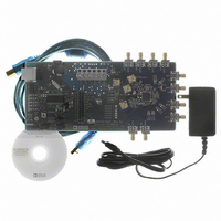
AD9520-1/PCBZ Analog Devices Inc, AD9520-1/PCBZ Datasheet

AD9520-1/PCBZ
Specifications of AD9520-1/PCBZ
Related parts for AD9520-1/PCBZ
AD9520-1/PCBZ Summary of contents
Page 1
... VCO (such as VCO calibration) can be ignored. This document covers the AD9520 family. The which is identical to the AD9520 except that it has LVDS outputs, is covered in UG-077. For convenience, detailed information from the AD9520 data sheet has been included here. Use this user guide in conjunction with the AD9520 and AD9522 data sheet and software documentation available at www ...
Page 2
... VCO Calibration Window ........................................................ 11 Channel Divider Window ......................................................... 11 Output Driver Window ............................................................. 12 Debug Window ........................................................................... 12 Evaluation Software Menu Items.................................................. 13 Menu Bar ..................................................................................... 13 AD9520 PLL Loop Filter ............................................................... 14 Using the Evaluation Board to Program an AD9520 on a Customer Board .............................................................................. 15 AD9520 Binary File Generation ................................................... 16 Checksum Generation ............................................................... 16 Avoiding Checksum Mismatches ............................................. 16 ESD Caution................................................................................ 16 Rev Page ...
Page 3
... If the user wishes to connect a signal to REF2, connect that signal to the J13 SMA connector. DC-coupling is recommended in applications requiring automatic hitless reference switching. There is a possibility that the AD9520 receive buffer can chatter when an ac-coupled clock stops toggling. Connect an oscilloscope, spectrum analyzer, or other lab equipment to any of the SMA connectors on the right side of the board ...
Page 4
... I/O menu (see Figure 24), and select Ezssp-0, Ezssp-1, or Ezssp-2. Figure 3. Select USB Device Window See the Evaluation Software Components section for a description of the evaluation software features, or the Quick Start Guide to the AD9520 PLL section for details on the individual blocks of the AD9520. Rev Page ...
Page 5
... This quick start guide covers only simple PLL operation to start the PLL. See the AD9520 data sheet and Evaluation Software Components section for a detailed explanation of the various AD9520 features. The following case is an example for the AD9520-4 using the values in Table 1. Table 1. Parameter ...
Page 6
... Set the channel dividers by clicking DIVIDER 0 through DIVIDER 3, and entering the divider ratio. 13. Click the flashing red WRITE button under the REGISTER W/R section. This loads the desired settings to the AD9520 evaluation board. 14. Click the blinking yellow Cal VCO button to load the VCO calibration window ...
Page 7
... EVALUATION SOFTWARE COMPONENTS MAIN WINDOW The AD9520 evaluation software is composed of subsections that correspond to the major functional blocks of the AD9520. These subsections are listed in the following sections, and each of these has its own window. From the main window, each functional block can be accessed by clicking that block in the main window ...
Page 8
... There are many useful diagnostic signals available at these pins. The R divider output is particularly useful. In the example used in the Quick Start Guide to the AD9520 PLL section, the 80 kHz signal is visible on the STATUS pin to ensure that the reference inputs and R divider are working properly. ...
Page 9
... The EEPROM pin is pulled high by placing the S4 EEPROM jumper (located in the lower left corner of the evaluation board) across the center and right (high) pin. You can reset the AD9520 by clicking the red RESET button in the lower left corner of the main window, and selecting Strobe ResetB. ...
Page 10
... Norm Op. Figure 14. Reference Divider Window The various modes of the N divider are described in detail in the AD9520 data sheet. For most applications, the 8/9 or 16/17 dual modulus modes are used. For applications requiring a divider value larger than 131119, the 32/33 mode is provided. ...
Page 11
... The window also has a check box for setting the charge pump voltage to V /2, which is very useful for debugging the PLL and CP isolating the output driver section of the AD9520 from the PLL section. ZERO DELAY WINDOW The Zero Delay window shown in Figure 18 is accessed by clicking the ZERO DELAY box on the main window ...
Page 12
UG-076 OUTPUT DRIVER WINDOW The output driver window shown in Figure 22 is accessed by clicking any of the numbered triangular output driver symbols on the right side of the main window (see Figure 21). Figure 21. Driver Symbol Figure ...
Page 13
... The file menu has the following options: Load Setup Selecting Load Setup loads a previously saved AD9520 setup file (.stp). A setup file is a text file that contains the AD9520 register setup file, plus any evaluation board settings. Note that you must still perform a VCO calibration. ...
Page 14
... AD9520. However, the AD9516, AD9520, and AD9522 share R1 the same loop dynamics. Therefore, ADIsimCLK Version 1 can also be used for modeling the AD9520 loop filter by selecting the corresponding version of the AD9516. ADIsimCLK is available at www.analog.com/clocks. Table 2 shows the correspondence between the components shown in Figure 27 and those on the evaluation board, as well as the default values ...
Page 15
... Evaluation Board User Guide USING THE EVALUATION BOARD TO PROGRAM AN AD9520 ON A CUSTOMER BOARD This guide shows how to use an AD9520 evaluation board to program an AD9520 on a customer board via the I It assumes that the user has access to the I on the target board, and knows the assigned address of the ...
Page 16
... The evaluation software automatically sets the VCO calibration now bit (Register 0x018[0]) in the .bin file if the PLL is turned on. If the VCO calibration now bit is not set, the AD9520 will be unable to lock the PLL after automatically loading the register values from the EEPROM without further user intervention. ...


