AD9520-1/PCBZ Analog Devices Inc, AD9520-1/PCBZ Datasheet - Page 11
AD9520-1/PCBZ
Manufacturer Part Number
AD9520-1/PCBZ
Description
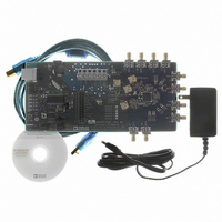
BOARD EVAL FOR AD9520-1
Manufacturer
Analog Devices Inc
Specifications of AD9520-1/PCBZ
Design Resources
Synchronizing Multiple AD9910 1 GSPS Direct Digital Synthesizers (CN0121) Phase Coherent FSK Modulator (CN0186)
Main Purpose
Timing, Clock Generator
Embedded
No
Utilized Ic / Part
AD9520-1
Primary Attributes
12 LVPECL/24 CMOS Output Clock Generator with 2.5 GHz VCO
Secondary Attributes
SPI and I2C Compatible Control Port
Silicon Manufacturer
Analog Devices
Application Sub Type
PLL Clock Synthesizer
Kit Application Type
Clock & Timing
Silicon Core Number
AD9520-0, AD9520-2, AD9520-2
Silicon Family Name
AD9520-X
Rohs Compliant
Yes
Lead Free Status / RoHS Status
Lead free / RoHS Compliant


Evaluation Board User Guide
CHARGE PUMP SETUP WINDOW
The Charge Pump Setup window shown in Figure 17 is
accessed by clicking the CHARGE PUMP box on the main
window.
This window is most often used to vary the charge pump
current.
The window also has a check box for setting the charge pump
voltage to V
isolating the output driver section of the AD9520 from the PLL
section.
ZERO DELAY WINDOW
The Zero Delay window shown in Figure 18 is accessed by
clicking the ZERO DELAY box on the main window.
When internal zero delay mode is selected, the window shrinks
because only Divider 0 can operate in the internal zero delay mode.
CP
/2, which is very useful for debugging the PLL and
Figure 17. Charge Pump Setup Window
Figure 18. Zero Delay Window
Rev. 0 | Page 11 of 16
VCO CALIBRATION WINDOW
The Calibrate VCO window shown in Figure 19 is accessed by
clicking the Cal VCO button on the main window.
A valid reference input signal must be present to complete
VCO calibration, and the VCO must be recalibrated any time
the VCO frequency changes by more than 40 MHz.
A VCO divider of 16 is suitable for all applications. However,
for applications where the phase detector frequency is <12 MHz,
using a smaller VCO calibration divider reduces calibration
time. Refer to the AD9520 data sheet for more details.
CHANNEL DIVIDER WINDOW
The channel divider window shown in Figure 20 is accessed by
clicking the appropriate channel divider. It is usually sufficient
to change only the divide ratio because the evaluation software
and the AD9520 duty cycle correction feature ensure that the
output duty cycle remains very close to 50%.
You can also vary the phase offset by changing the Phase Offset
Bits setting. However, for the new phase to take effect, the SYNC
signal must be toggled via the SYNC button in the lower left
corner of the main window.
Figure 20. Channel Divider Window
Figure 19. Calibrate VCO Window
UG-076
Related parts for AD9520-1/PCBZ
Image
Part Number
Description
Manufacturer
Datasheet
Request
R

Part Number:
Description:
12/24 Channel Clock Gen 2,0GH
Manufacturer:
Analog Devices Inc
Datasheet:

Part Number:
Description:
12/24 Channel Clock Gen 2,0GH
Manufacturer:
Analog Devices Inc
Datasheet:
Part Number:
Description:
12/24 Channel Clock Gen 2,0GH
Manufacturer:
Analog Devices Inc
Datasheet:
Part Number:
Description:
12/24 Channel Clock Gen 2,0GH
Manufacturer:
Analog Devices Inc
Datasheet:
Part Number:
Description:
12/24 Channel Clock Gen 2,0GH
Manufacturer:
Analog Devices Inc
Datasheet:
Part Number:
Description:
Clock IC With 2.8GHz On-chip VCO
Manufacturer:
Analog Devices Inc
Datasheet:
Part Number:
Description:
Lock IC With 2.8GHz On-chip VCO
Manufacturer:
Analog Devices Inc
Datasheet:
Part Number:
Description:
12/24 Channel Clock Gen 2,5 GHz VCO
Manufacturer:
Analog Devices Inc
Datasheet:
Part Number:
Description:
12/24 Channel Clock Distribution W/ On-C
Manufacturer:
Analog Devices Inc
Datasheet:
Part Number:
Description:
12/24 Channel Clock Gen 2,25GH
Manufacturer:
Analog Devices Inc
Datasheet:
Part Number:
Description:
12/24 Channel Clock Distribution W/ On-C
Manufacturer:
Analog Devices Inc
Datasheet:
Part Number:
Description:
12/24 Channel Clock Distribution W/ On-C
Manufacturer:
Analog Devices Inc
Datasheet:
Part Number:
Description:
Clock IC With 1.6GHz On-chip VCO
Manufacturer:
Analog Devices Inc
Datasheet:
Part Number:
Description:
Clock IC With 1.6GHz On-chip VCO
Manufacturer:
Analog Devices Inc
Datasheet:
Part Number:
Description:
12/24-Output Clock Generator
Manufacturer:
Analog Devices Inc
Datasheet: