ADCLK950/PCBZ Analog Devices Inc, ADCLK950/PCBZ Datasheet
ADCLK950/PCBZ
Specifications of ADCLK950/PCBZ


Related parts for ADCLK950/PCBZ


ADCLK950/PCBZ Summary of contents
Page 1
FEATURES FEATURES 2 selectable differential inputs 2 selectable differential inputs 4.8 GHz operating frequency 4.8 GHz operating frequency 75 fs rms broadband random jitter 75 fs rms broadband random jitter On-chip input terminations On-chip input terminations 3.3 V power supply ...
Page 2
ADCLK950 TABLE OF CONTENTS Features .............................................................................................. 1 Applications ....................................................................................... 1 General Description ......................................................................... 1 Functional Block Diagram .............................................................. 1 Revision History ............................................................................... 2 Specifications ..................................................................................... 3 Electrical Characteristics ............................................................. 3 Absolute Maximum Ratings ............................................................ 5 Determining Junction Temperature .......................................... 5 ...
Page 3
SPECIFICATIONS ELECTRICAL CHARACTERISTICS Typical (Typ column) values are given for V (Max column) values are given over the full V Table 1. Clock Inputs and Outputs Parameter Symbol DC INPUT CHARACTERISTICS Input Common Mode Voltage V ICM Input Differential Range ...
Page 4
ADCLK950 Table 3. Input Select Control Pin Parameter Logic 1 Voltage Logic 0 Voltage Logic 1 Current Logic 0 Current Capacitance Table 4. Power Parameter POWER SUPPLY Supply Voltage Requirement Power Supply Current Negative Supply Current Positive Supply Current Power ...
Page 5
ABSOLUTE MAXIMUM RATINGS Table 5. Parameter Supply Voltage V − Input Voltage CLK0, CLK1, CLK0, CLK1, IN_SEL CLK0, CLK1, CLK0, CLK1 Pin (CML, T LVPECL Termination) CLK0, CLK1 to CLK0, CLK1 Input Termination, V ...
Page 6
ADCLK950 PIN CONFIGURATION AND FUNCTION DESCRIPTIONS Table 7. Pin Function Descriptions Pin No. Mnemonic Description 1 IN_SEL Input Select. Logic 0 selects CLK0 and CLK0 inputs. Logic 1 selects CLK1 and CLK1 inputs. 2 CLK0 Differential Input (Positive ...
Page 7
TYPICAL PERFORMANCE CHARACTERISTICS ICM REF 100mV/DIV Figure 3. LVPECL Output Waveform @ 200 MHz 1.8 1.7 1.6 1.5 1.4 1.3 1.2 ...
Page 8
ADCLK950 1.56 1.54 –40°C 1.52 +25°C 1.50 1.48 +85°C 1.46 1.44 1.42 2.75 2.85 2.95 3.05 3.15 3.25 3.35 POWER SUPPLY (V) Figure 9. Differential Output Voltage Swing vs. Power Supply Voltage vs. Temperature 1.6 V p-p ID ...
Page 9
FUNCTIONAL DESCRIPTION CLOCK INPUTS The ADCLK950 accepts a differential clock input from one of two inputs and distributes the selected clock to all 10 LVPECL outputs. The maximum specified frequency is the point at which the output voltage swing is ...
Page 10
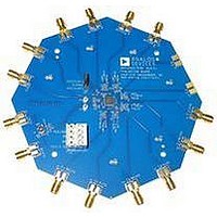
... ADCLK950. The PCB attachment must provide a good thermal path to a larger heat dissipation area. This requires a grid of vias from the top layer down to the V The ADCLK950 evaluation board (ADCLK950/PCBZ) provides an example of how to attach the part to the PCB. VIAS TO V Figure 18. PCB Land for Attaching Exposed Paddle Rev ...
Page 11
INPUT TERMINATION OPTIONS REF 50Ω 50Ω CLKx CLKx ADCLK950 CONNECT Figure 19. DC-Coupled CML Input Termination REF 0.01µF (OPTIONAL 50Ω ...
Page 12
... ORDERING GUIDE Model 1 Temperature Range ADCLK950BCPZ −40°C to +85°C ADCLK950BCPZ-REEL7 −40°C to +85°C ADCLK950/PCBZ RoHS Compliant Part. ©2009–2010 Analog Devices, Inc. All rights reserved. Trademarks and registered trademarks are the property of their respective owners. 6.00 BSC SQ 0.60 MAX ...