ADNK-5053-HT01 Avago Technologies US Inc., ADNK-5053-HT01 Datasheet - Page 9
ADNK-5053-HT01
Manufacturer Part Number
ADNK-5053-HT01
Description
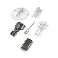
KIT REF DESIGN OPT MOUSE A5050
Manufacturer
Avago Technologies US Inc.
Specifications of ADNK-5053-HT01
Main Purpose
Reference Design, Optical Mouse
Utilized Ic / Part
ADNS-5050
Description/function
Optical Mouse Sensor Kit
Interface Type
USB
Product
Display Modules
Touch Panel
No Touch Panel
For Use With/related Products
HT82M99E
Lead Free Status / RoHS Status
Lead free / RoHS Compliant
Secondary Attributes
-
Embedded
-
Primary Attributes
-
Lead Free Status / Rohs Status
Lead free / RoHS Compliant


AC Electrical Specifications
Electrical Characteristics over recommended operating conditions. Typical values at 25 °C, V
Parameter
Power Down
Wake from Power Down
Reset Pulse Width
Motion Delay after Reset
SDIO Rise Time
SDIO Fall Time
SDIO delay after SCLK
SDIO Hold Time
SDIO Setup Time
SPI Time between
Write Commands
SPI Time between Write
and Read Commands
SPI Time between
Read and Subsequent
Commands
SPI Read Address-Data
Delay
NCS Inactive after
Motion Burst
NCS to SCLK Active
SCLK to NCS Inactive
(for read operation)
SCLK to NCS Inactive
(for write operation)
NCS to SDIO High-Z
Transient Supply Current
9
Symbol
t
t
t
t
t
t
t
t
t
t
t
t
t
t
t
t
t
t
t
I
DDT
PD
WAKEUP
RESET
MOT-RST
r-SDIO
f-SDIO
DLY-SDIO
hold-SDIO
setup-SDIO
SWW
SWR
SRW
SRR
SRAD
BEXIT
NCS-SCLK
SCLK-NCS
SCLK-NCS
NCS-SDIO
Minimum
50
250
100
120
30
20
500
4
250
120
120
20
Typical
150
150
Maximum
50
55
50
300
300
120
10
500
60
Units
ms
ms
ns
ms
ns
ns
ns
ns
ns
µs
µs
ns
µs
ns
ns
ns
us
ns
mA
Notes
From PD (when bit 1 of register 0x0d
is set) to low current
From PD inactive (when NRESET pin is
asserted high or write 0x5a to register
0x3a) to valid motion
Active low.
From NRESET pull high to valid mo
tion, assuming V
present.
C
C
From SCLK falling edge to SDIO data
valid, no load conditions.
Data held until next falling SCLK edge.
From data valid to SCLK rising edge.
From rising SCLK for last bit of the first
data byte, to rising SCLK for last bit of
the second data byte.
From rising SCLK for last bit of the first
data byte, to rising SCLK for last bit of
the second address byte.
From rising SCLK for last bit of the first
data byte, to falling SCLK for the first
bit of the next address.
From rising SCLK for last bit of the
address byte, to falling SCLK for first bit
of data being read.
Minimum NCS inactive time after
motion burst before next SPI usage.
From NCS falling edge to first SCLK
rising edge.
From last SCLK rising edge to NCS
rising edge, for valid SDIO data
transfer.
From last SCLK rising edge to NCS
rising edge, for valid SDIO data transfer.
From NCS rising edge to SDIO high-Z
state.
Max supply current during a V
from 0 to V
L
L
= 100pF
= 100pF
DD
DD
= 5.0 V.
.
DD
and motion is
DD
ramp
Related parts for ADNK-5053-HT01
Image
Part Number
Description
Manufacturer
Datasheet
Request
R

Part Number:
Description:
A2700 Sample Kit
Manufacturer:
Avago Technologies US Inc.
Datasheet:

Part Number:
Description:
OPTOCOUPLER GATE DRV 2A 16-SOIC
Manufacturer:
Avago Technologies US Inc.
Datasheet:
Part Number:
Description:
OPTOCOUPLER 2CH 2.5A 16-SOIC
Manufacturer:
Avago Technologies US Inc.
Datasheet:

Part Number:
Description:
OPTOCOUPLER GATE DRV 0.4A 16SOIC
Manufacturer:
Avago Technologies US Inc.
Datasheet:

Part Number:
Description:
OPTOCOUPLER 2.0A 250KHZ 8-DIP
Manufacturer:
Avago Technologies US Inc.
Datasheet:

Part Number:
Description:
OPTOCOUPLER 2.0A 250KHZ GW 8-SMD
Manufacturer:
Avago Technologies US Inc.
Datasheet:

Part Number:
Description:
OPTOCOUPLER 2CH 15MBD 3.3V 8SOIC
Manufacturer:
Avago Technologies US Inc.
Datasheet:
Part Number:
Description:
OPTOCOUPLER DARL-OUT 8-DIP
Manufacturer:
Avago Technologies US Inc.
Datasheet:
Part Number:
Description:
OPTOCOUPLER IGBT DRIVE 0.4A 8DIP
Manufacturer:
Avago Technologies US Inc.
Datasheet:
Part Number:
Description:
OPTOCOUPLER DARL-OUT 8-DIP
Manufacturer:
Avago Technologies US Inc.
Datasheet:

Part Number:
Description:
OPTOCOUPLER 1CH 1MBS 8-SMD GW
Manufacturer:
Avago Technologies US Inc.
Datasheet:
Part Number:
Description:
OPTOCOUPLER GATE DRIVER 8-DIP
Manufacturer:
Avago Technologies US Inc.
Datasheet:

Part Number:
Description:
OPTOCOUPLER GATE DRIVER 8-SMD
Manufacturer:
Avago Technologies US Inc.
Datasheet:

Part Number:
Description:
OPTOCOUPLER PHOTOTRANS 4-SMD
Manufacturer:
Avago Technologies US Inc.
Datasheet:

Part Number:
Description:
OPTOCOUPLER W/BASE 6-DIP
Manufacturer:
Avago Technologies US Inc.
Datasheet: