EVAL-ADM1063TQEBZ Analog Devices Inc, EVAL-ADM1063TQEBZ Datasheet - Page 4
EVAL-ADM1063TQEBZ
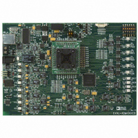
Manufacturer Part Number
EVAL-ADM1063TQEBZ
Description
BOARD EVALUATION FOR ADM1063TQ
Manufacturer
Analog Devices Inc
Specifications of EVAL-ADM1063TQEBZ
Main Purpose
Power Management, Power Supply Supervisor/Tracker/Sequencer
Embedded
No
Utilized Ic / Part
ADM1063
Primary Attributes
10 Channel Supervisor / Sequencer, 6 Voltage Output DACs
Secondary Attributes
GUI Programmable via SMBus (via USB)
Lead Free Status / RoHS Status
Lead free / RoHS Compliant


ADM1063
SPECIFICATIONS
VH = 3.0 V to 14.4 V
Table 1.
Parameter
POWER SUPPLY ARBITRATION
POWER SUPPLY
SUPPLY FAULT DETECTORS
ANALOG-TO-DIGITAL CONVERTER
VH, VPx
VPx
VH
VDDCAP
C
Supply Current, I
Additional Currents
ADC Supply Current
EEPROM Erase Current
VH Pin
VPx Pins
VXx Pins
Absolute Accuracy
Threshold Resolution
Digital Glitch Filter
Signal Range
Input Reference Voltage on REFIN Pin, V
Resolution
INL
Gain Error
VDDCAP
All PDO FET Drivers On
Current Available from VDDCAP
Input Impedance
Input Attenuator Error
Detection Ranges
Input Impedance
Input Attenuator Error
Detection Ranges
Input Impedance
Detection Range
High Range
Midrange
Midrange
Low Range
Ultralow Range
Ultralow Range
VH
, I
1
VPx
, VPx = 3.0 V to 6.0 V
REFIN
1
, T
Min
3.0
2.7
10
6
2.5
2.5
1.25
0.573
1
0.573
0
A
= −40°C to +85°C, unless otherwise noted.
Typ
4.75
4.2
1
1
10
52
±0.05
52
±0.05
8
0
100
2.048
12
Rev. B | Page 4 of 32
Max
6.0
14.4
5.4
6
2
14.4
6
6
3
1.375
1.375
±1
V
±2.5
±0.05
REFIN
mA
Unit
V
V
V
V
μF
mA
mA
mA
mA
kΩ
%
V
V
kΩ
%
V
V
V
MΩ
V
%
Bits
μs
μs
V
V
Bits
LSB
%
Test Conditions/Comments
Minimum supply required on one of VH, VPx
Maximum VDDCAP = 5.1 V, typical
VDDCAP = 4.75 V
Regulated LDO output
Minimum recommended decoupling capacitance
VDDCAP = 4.75 V, PDO1 to PDO10 off, ADC off
VDDCAP = 4.75 V, PDO1 to PDO6 loaded with 1 μA
each, PDO7 to PDO10 off
Maximum additional load that can be drawn from all
PDO pull-ups to VDDCAP
Running round-robin loop
1 ms duration only, VDDCAP = 3 V
Midrange and high range
Low range and midrange
No input attenuation error
No input attenuation error
VREF error + DAC nonlinearity + comparator offset error
+ input attenuation error
Minimum programmable filter length
Maximum programmable filter length
The ADC can convert signals presented to the VH, VPx,
and VXx pins; VPx and VH input signals are attenuated
depending on the selected range; a signal at the pin
corresponding to the selected range is from 0.573 V to
1.375 V at the ADC input
Endpoint corrected, V
V
REFIN
= 2.048 V
REFIN
= 2.048 V
Related parts for EVAL-ADM1063TQEBZ
Image
Part Number
Description
Manufacturer
Datasheet
Request
R

Part Number:
Description:
IC, ADJ LDO REG, 1.5V TO 5V 250mA MSOP-8
Manufacturer:
Vishay
Datasheet:

Part Number:
Description:
IC, ADJ LDO REG, 1.5V TO 5V 0.6A 8-TSSOP
Manufacturer:
Vishay
Datasheet:
Part Number:
Description:
IC, ADJ LDO REG, 1.5V TO 5V 250mA MSOP-8
Manufacturer:
Vishay
Datasheet:

Part Number:
Description:
IC ADJ LDO REG 1.5V TO 5V 150mA 5-SOT-23
Manufacturer:
Vishay
Datasheet:

Part Number:
Description:
BOARD EVAL AS1324-AD
Manufacturer:
austriamicrosystems
Datasheet:
Part Number:
Description:
IC, ADJ LDO REG, 1.5V TO 5V 0.6A 8-TSSOP
Manufacturer:
Vishay
Datasheet:

Part Number:
Description:
IC, ADJ LDO REG, 1.5V TO 5V, 0.3A, MSOP8
Manufacturer:
Vishay
Datasheet:
Part Number:
Description:
IC, ADJ LDO REG, 1.5V TO 5V, 0.3A, MSOP8
Manufacturer:
Vishay
Datasheet:
Part Number:
Description:
IC, ADJ LDO REG 1.215V TO 5V 0.3A MSOP-8
Manufacturer:
Vishay
Datasheet:
Part Number:
Description:
IC, ADJ LDO REG 1.215V TO 5V 0.3A MSOP-8
Manufacturer:
Vishay
Datasheet:

Part Number:
Description:
±1.7g Dual-Axis IMEMS Accelerometer Evaluation Board
Manufacturer:
Analog Devices Inc
Datasheet:

Part Number:
Description:
IC MULTIPLIER ANALOG 8-SOIC T/R
Manufacturer:
Analog Devices Inc
Datasheet:

Part Number:
Description:
IC ANALOG MULTIPLIER 8-DIP
Manufacturer:
Analog Devices Inc
Datasheet:
Part Number:
Description:
IC ANALOG MULTIPLIER 8-SOIC
Manufacturer:
Analog Devices Inc
Datasheet:
Part Number:
Description:
IC ANALOG MULTIPLIER 8-DIP
Manufacturer:
Analog Devices Inc
Datasheet: