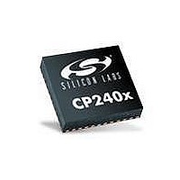
CP2400AB Silicon Laboratories Inc, CP2400AB Datasheet - Page 17

CP2400AB
Manufacturer Part Number
CP2400AB
Description
BOARD EVAL SPI LCD DRIVER CP2400
Manufacturer
Silicon Laboratories Inc
Specifications of CP2400AB
Main Purpose
LCD Development
Embedded
No
Utilized Ic / Part
CP2400
Primary Attributes
I²C, SMBus Interfaces
Secondary Attributes
Up to 128 segments
Product
Microcontroller Accessories
Core Processor
CP2400
Clock Speed
20 MHz
Interface Type
SPI
Timers
2
Operating Supply Voltage
1.8 V to 3.6 V
Cpu Core
CP2400
Lead Free Status / RoHS Status
Contains lead / RoHS non-compliant
Lead Free Status / RoHS Status
Lead free / RoHS Compliant, Contains lead / RoHS non-compliant
Other names
336-1857
CP2400/1-DK
7.2.4. Measuring Current
The header (J17) and terminal block (H2) provide a way to measure the total supply current flowing from the power
supply source to the MCU. The measured current does not include any current from the VBAT LED (DS2), the
address latch (U4) or the quiescent current from the power supply; however, it does include the current used by
any LEDs powered from the VDD/DC+ supply net or sourced through a GPIO pin. See the target board schematics
in Figures 19 through 21 for additional information.
7.3. System Clock Sources
7.3.1. Internal Oscillators
The C8051F930 device installed on the target board features a factory calibrated programmable high-frequency
internal oscillator (24.5 MHz base frequency, ±2%) and a low power internal oscillator (20 MHz ±10%). After each
reset, the low power oscillator divided by 8 results in a default system clock frequency of 2.5 MHz (±10%). The
selected system clock and the system clock divider may be configured by software for operation at other
frequencies. For low-frequency operation, the C8051F930 features a smaRTClock real time clock. A 32.768 kHz
Watch crystal (Y2) is included on the target board. If you wish to operate the C8051F930 device at a frequency not
available with the internal oscillators, an external crystal may be used. Refer to the C8051F93x-C8051F92x data
sheet for more information on configuring the system clock source.
7.3.2. External Oscillator Options
The target board is designed to facilitate the installation of an external crystal (Y1). Install a 10 M resistor at R9
and install capacitors at C20 and C21 using values appropriate for the crystal you select. If you wish to operate the
external oscillator in capacitor or RC mode, options to install a capacitor or an RC network are also available on the
target board. Populate C21 for capacitor mode, and populate R16 and C21 for RC mode. Refer to the C8051F93x-
C8051F92x data sheet for more information on the use of external oscillators.
7.4. Port I/O Headers (J2, J3, J4, J6)
Access to all Port I/O on the C8051F930 is provided through the headers J2, J3, and J4. The header J6 provides
access to the ground plane for easy clipping of oscilloscope probes.
7.5. Switches and LEDs
Three push-button switches are provided on the target board. Switch SW1 is connected to the reset pin of the
C8051F930. Pressing SW1 puts the device into its hardware-reset state. Switches SW2 and SW3 are connected to
the C8051F930’s general purpose I/O (GPIO) pins through headers. Pressing SW2 or SW3 generates a logic low
signal on the port pin. Remove the shorting block from the header (J8) to disconnect the switches from the port
pins. The port pin signal is also routed to pins on the J2 and P1 I/O connectors. See Table 1 for the port pins and
headers corresponding to each switch.
Two touch sensitive (contactless) switches are provided on the target board. The operation of these switches
require appropriate firmware running on the C8051F930 MCU that can sense the state of the switch. See Section
6.3. "Touch Sensitive Switch Example‚" on page 11 for details about example source code.
Five power LEDs are provided on the target board to serve as indicators. Each of the two regulators has a red LED
used to indicate the presence of power at the output of the regulator. A red USB Power LED turns on when a USB
cable is plugged into the USB connector P3. One power LED is also added to each of the two primary supply nets
powering the MCU (VDD/DC+ and VBAT). The LEDs connected to the supply nets may be disabled by removing
the shorting blocks from J1 and J5.
Two LEDs are connected to GPIO pins P1.5 and P1.6 for use by application software. See Table 1 for the port pins
and headers corresponding to each LED.
A potentiometer (R15) is also provided on the target board for generating analog signals. Place a shorting block on
J16 to connect the wiper to P0.6/CNVSTR. The header J15 allows the negative terminal of the potentiometer to be
tied to GND or to P1.4. When tied to GND, the potentiometer is always enabled and will draw a measurable
amount of supply current. When tied to P1.4, it only draws current when P1.4 is driving a logic 0 and draws no
current when P1.4 is driving a logic 1.
Rev. 0.1
17


