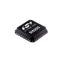
SI5325/26-EVB Silicon Laboratories Inc, SI5325/26-EVB Datasheet - Page 6

SI5325/26-EVB
Manufacturer Part Number
SI5325/26-EVB
Description
BOARD EVAL FOR SI5325/26
Manufacturer
Silicon Laboratories Inc
Specifications of SI5325/26-EVB
Main Purpose
Timing, Clock Generator
Utilized Ic / Part
SI5325, SI5326
Processor To Be Evaluated
Si5325 and Si5326
Lead Free Status / RoHS Status
Lead free / RoHS Compliant
Secondary Attributes
-
Embedded
-
Primary Attributes
-
Lead Free Status / Rohs Status
Lead free / RoHS Compliant
Si5326
6
Table 2. DC Characteristics (Continued)
(V
Differential Output
Swing
Single Ended Output
Swing
Differential Output
Voltage
Common Mode Output
Voltage
Differential Output
Voltage
Common Mode Output
Voltage
Differential Output
Resistance
Output Voltage Low
Output Voltage High
Notes:
DD
1.
2. No under- or overshoot is allowed.
3. LVPECL outputs require nominal V
4. This is the amount of leakage that the 3-Level inputs can tolerate from an external driver. See Si53xx
5. LVPECL, CML, LVDS and low-swing LVDS measured with Fo = 622.08 MHz.
= 1.8 ± 5%, 2.5 ±10%, or 3.3 V ±10%, T
Parameter
Current draw is independent of supply voltage
Family Reference Manual for more details.
CKO
CKO
CKO
CKO
CKO
Symbol
CKO
CKO
CKO
CKO
VOHLH
VOLLH
VCM
VCM
VSE
VD
VD
VD
RD
LVPECL 100 load line-
LVPECL 100 load line-
LVDS 100 load line-to-
CML 100 load line-to-
CML 100 load line-to-
A
100 load line-to-line
100 load line-to-line
CML, LVPECL, LVDS
= –40 to 85 °C)
DD
Low Swing LVDS
Test Condition
≥ 2.5 V.
V
DD
CMOS
CMOS
to-line
to-line
LVDS
line
line
line
= 1.71 V
Rev. 1.0
1.125
0.8 x
V
Min
350
500
350
1.1
0.5
—
—
—
DD
V
DD
Typ
425
700
425
200
1.2
—
—
—
—
-0.36
1.275
Max
0.93
500
900
500
1.9
0.4
—
—
—
mV
mV
mV
Unit
V
V
V
V
V
V
PP
PP
PP
PP
PP


