MCP3421EV Microchip Technology, MCP3421EV Datasheet - Page 13
MCP3421EV
Manufacturer Part Number
MCP3421EV
Description
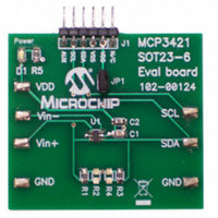
BOARD EVAL FOR MCP3421 SOT23-6
Manufacturer
Microchip Technology
Specifications of MCP3421EV
Design Resources
MCP3421EV Gerber Files
Number Of Adc's
1
Number Of Bits
18
Sampling Rate (per Second)
4
Data Interface
Serial
Inputs Per Adc
1 Single Ended
Input Range
±2.5 V
Voltage Supply Source
Single Supply
Operating Temperature
-40°C ~ 125°C
Utilized Ic / Part
MCP3421
Silicon Manufacturer
Microchip
Application Sub Type
ADC
Kit Application Type
Data Converter
Silicon Core Number
MCP3421
Kit Contents
Board
Rohs Compliant
Yes
Lead Free Status / RoHS Status
Not applicable / Not applicable
Available stocks
Company
Part Number
Manufacturer
Quantity
Price
Company:

Part Number:
MCP3421EV
Manufacturer:
Microchip Technology
Quantity:
135


4.9
4.9.1
The digital output code is proportional to the input
voltage and PGA settings. The output data format is a
binary two’s complement. With this code scheme, the
MSB can be considered a sign indicator. When the
MSB is a logic ‘0’, the input is positive. When the MSB
is a logic ‘1’, the input is negative. The following is an
example of the output code:
a.
b.
c.
The MSB (sign bit) is always transmitted first through
the I
conversion is 18, 16, 14, or 12 bits depending on the
conversion rate selection bit settings by the user.
The output codes will not roll-over even if the input volt-
age exceeds the maximum input range. In this case,
the code will be locked at 0111...11 for all voltages
greater than (V
voltages less than -V
example of output codes of various input levels for 18
bit conversion mode.
minimum and maximum output codes for each
conversion rate option.
The number of output code is given by:
EQUATION 4-2:
The LSB of the data conversion is given by:
EQUATION 4-3:
© 2009 Microchip Technology Inc.
Number of Output Code
Where:
Where:
for a negative full scale input voltage:
100...000
Example: (V
for a zero differential input voltage: 000...000
Example: (V
for
011...111
Example: (V
2
=
N = User programmable bit resolution:
See
C serial data line. The resolution for each
(
Digital Output Codes and
Conversion to Real Values
Maximum Code
a
Table 4-3
DIGITAL OUTPUT CODE FROM
DEVICE
LSB
12,14,16, or 18
positive
REF
IN
IN
IN
=
+ - V
+ - V
+ - V
- 1 LSB)/PGA and 1000...00 for
2 V
--------------------- -
for Maximum Code.
×
Table 4-3
REF
2
IN
IN
IN
full
N
+
REF
-)
-) = 0
-)
1
/PGA.
•
•
) PGA
PGA = -2.048V
PGA = 2.048V
×
scale
=
2 2.048V
--------------------------
shows an example of
Table 4-2
×
×
2
input
N
(
---------------------------------- -
V
IN
2.048V
+ V
voltage:
shows an
–
IN
-
)
Table 4-1
setting. The measured unknown input voltage is
obtained by multiplying the output codes with LSB. See
the following section for the input voltage calculation
using the output codes.
TABLE 4-1:
TABLE 4-2:
TABLE 4-3:
Note 1:
Resolution
Note:
[V
Setting
Input Voltage:
IN
Resolution Setting
V
12
14
16
18
+ - V
2:
REF
< -V
-1 LSB
-2 LSB
≥
- V
2 LSB
1 LSB
shows the LSB size of each conversion rate
V
- 1 LSB
MSB is a sign indicator:
0: Positive input (V
1: Negative input (V
Output data format is binary two’s
complement.
IN
0
Maximum n-bit code = 2
Minimum n-bit code = -1 x 2
REF
REF
12 bits
14 bits
16 bits
18 bits
REF
-] • PGA
Data Rate
3.75 SPS
240 SPS
60 SPS
15 SPS
RESOLUTION SETTINGS VS.
LSB
EXAMPLE OF OUTPUT CODE
FOR 18 BITS (NOTE 1,NOTE 2)
MINIMUM AND MAXIMUM
OUTPUT CODES (NOTE)
011111111111111111
011111111111111111
000000000000000010
000000000000000001
000000000000000000
111111111111111111
111111111111111110
100000000000000000
100000000000000000
Minimum
Digital Output Code
-131072
-32768
MCP3421
-2048
-8192
IN
Code
IN
+ > V
+ < V
N-1
DS22003E-page 13
15.625 µV
IN
IN
62.5 µV
250 µV
-)
- 1
N-1
1 mV
-)
LSB
Maximum
131071
32767
Code
8191
2047
Related parts for MCP3421EV
Image
Part Number
Description
Manufacturer
Datasheet
Request
R

Part Number:
Description:
Manufacturer:
Microchip Technology Inc.
Datasheet:
Part Number:
Description:
Manufacturer:
Microchip Technology Inc.
Datasheet:
Part Number:
Description:
Manufacturer:
Microchip Technology Inc.
Datasheet:
Part Number:
Description:
Manufacturer:
Microchip Technology Inc.
Datasheet:
Part Number:
Description:
Manufacturer:
Microchip Technology Inc.
Datasheet:
Part Number:
Description:
Manufacturer:
Microchip Technology Inc.
Datasheet:
Part Number:
Description:
Manufacturer:
Microchip Technology Inc.
Datasheet:
Part Number:
Description:
Manufacturer:
Microchip Technology Inc.
Datasheet: