MCP3421EV Microchip Technology, MCP3421EV Datasheet - Page 9
MCP3421EV
Manufacturer Part Number
MCP3421EV
Description
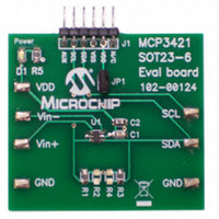
BOARD EVAL FOR MCP3421 SOT23-6
Manufacturer
Microchip Technology
Specifications of MCP3421EV
Design Resources
MCP3421EV Gerber Files
Number Of Adc's
1
Number Of Bits
18
Sampling Rate (per Second)
4
Data Interface
Serial
Inputs Per Adc
1 Single Ended
Input Range
±2.5 V
Voltage Supply Source
Single Supply
Operating Temperature
-40°C ~ 125°C
Utilized Ic / Part
MCP3421
Silicon Manufacturer
Microchip
Application Sub Type
ADC
Kit Application Type
Data Converter
Silicon Core Number
MCP3421
Kit Contents
Board
Rohs Compliant
Yes
Lead Free Status / RoHS Status
Not applicable / Not applicable
Available stocks
Company
Part Number
Manufacturer
Quantity
Price
Company:

Part Number:
MCP3421EV
Manufacturer:
Microchip Technology
Quantity:
135


3.0
The descriptions of the pins are listed in
TABLE 3-1:
3.1
V
MCP3421 device accepts a fully differential analog
input signal which is connected on the V
input pins. The differential voltage that is converted is
defined by V
applied at the V
at the V
V
differential and single-ended connection examples.
The input signal level is amplified by the programmable
gain amplifier (PGA) before the conversion. The
differential input voltage should not exceed an absolute
of (V
is the internal reference voltage (2.048V) and PGA is
the PGA gain setting. The converter output code will
saturate if the input range exceeds (V
The absolute voltage range on each of the differential
input pins is from V
above or below this range will cause leakage currents
through the Electrostatic Discharge (ESD) diodes at
the input pins. This ESD current can cause unexpected
performance of the device. The common mode of the
analog inputs should be chosen such that both the
differential analog input range and the absolute voltage
range on each pin are within the specified operating
range
Characteristics” and Section 4.0 “Description of
Device Operation”.
See Section 4.5 “Input Voltage Range” for more
details of the input voltage range.
Figure 3-1
device uses a switched capacitor input stage at the
front end. C
typically about 4 pF. D
C
© 2009 Microchip Technology Inc.
IN
SS
SAMPLE
MCP3421
+ and V
REF
for a single-ended operation. See
1
2
3
4
5
6
IN
/PGA) for accurate measurement, where V
PIN DESCRIPTIONS
is the differential input sampling capacitor.
Analog Inputs (V
- pin. The user can also connect V
defined
shows the input structure of the device. The
IN
IN
PIN
- are differential signal input pins. The
= (V
IN
is the package pin capacitance and
+ pin and V
PIN FUNCTION TABLE
IN
Symbol
SS
+ - V
V
SDA
SCL
V
V
V
in
-0.3V to V
IN
DD
IN
SS
1
+
-
and D
IN
-) where V
Section 1.0
IN
- is the voltage applied
2
IN
Positive Differential Analog Input Pin
Ground Pin
Serial Clock Input Pin of the I
Bidirectional Serial Data Pin of the I
Positive Supply Voltage Pin
Negative Differential Analog Input Pin
DD
are the ESD diodes.
+, V
+0.3V. Any voltage
IN
REF
IN
+ is the voltage
Table
Figure 6-4
-)
/PGA).
IN
“Electrical
+ and V
IN
3-1.
-
pin to
REF
IN
for
-
2
C Interface
3.2
V
requires an appropriate bypass capacitor of about
0.1 µF (ceramic) to ground. An additional 10 µF
capacitor (tantalum) in parallel is also recommended
to further attenuate high frequency noise present in
some application boards. The supply voltage (V
must be maintained in the 2.7V to 5.5V range for
specified operation.
V
device. The user must connect the V
plane through a low impedance connection. If an
analog ground path is available in the application PCB
(printed circuit board), it is highly recommended that
the V
isolated within an analog ground plane of the circuit
board.
3.3
SCL is the serial clock pin of the I
MCP3421 acts only as a slave and the SCL pin
accepts only external serial clocks. The input data
from the Master device is shifted into the SDA pin on
the rising edges of the SCL clock and output from the
MCP3421 occurs at the falling edges of the SCL clock.
The SCL pin is an open-drain N-channel driver.
Therefore, it needs a pull-up resistor from the V
to the SCL pin. Refer to Section 5.3 “I
Communications” for more details of I
Interface communication.
DD
SS
is the ground pin and the current return path of the
2
Description
is the power supply pin for the device. This pin
C Interface
SS
Supply Voltage (V
pin be tied to the analog ground path or
Serial Clock Pin (SCL)
MCP3421
DD
, V
SS
2
C interface. The
DS22003E-page 9
pin to a ground
SS
)
2
2
C Serial
C Serial
DD
line
DD
)
Related parts for MCP3421EV
Image
Part Number
Description
Manufacturer
Datasheet
Request
R

Part Number:
Description:
Manufacturer:
Microchip Technology Inc.
Datasheet:
Part Number:
Description:
Manufacturer:
Microchip Technology Inc.
Datasheet:
Part Number:
Description:
Manufacturer:
Microchip Technology Inc.
Datasheet:
Part Number:
Description:
Manufacturer:
Microchip Technology Inc.
Datasheet:
Part Number:
Description:
Manufacturer:
Microchip Technology Inc.
Datasheet:
Part Number:
Description:
Manufacturer:
Microchip Technology Inc.
Datasheet:
Part Number:
Description:
Manufacturer:
Microchip Technology Inc.
Datasheet:
Part Number:
Description:
Manufacturer:
Microchip Technology Inc.
Datasheet: