MCP3909EV-MCU16 Microchip Technology, MCP3909EV-MCU16 Datasheet - Page 28
MCP3909EV-MCU16
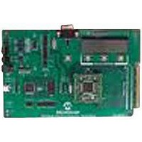
Manufacturer Part Number
MCP3909EV-MCU16
Description
EVALUATION BOARD FOR MCP3909
Manufacturer
Microchip Technology
Datasheets
1.MCP3909T-ISS.pdf
(44 pages)
2.MCP3909T-ISS.pdf
(104 pages)
3.MCP3909EV-MCU16.pdf
(38 pages)
Specifications of MCP3909EV-MCU16
Number Of Adc's
2
Number Of Bits
16
Sampling Rate (per Second)
15k
Data Interface
Serial
Inputs Per Adc
1 Differential
Input Range
±1 V
Voltage Supply Source
Analog and Digital
Operating Temperature
-40°C ~ 85°C
Utilized Ic / Part
MCP3909
Silicon Manufacturer
Microchip
Application Sub Type
ADC
Kit Application Type
Data Converter
Silicon Core Number
MCP3909
Kit Contents
Board
Lead Free Status / RoHS Status
Lead free / RoHS Compliant


MCP3909
5.4
This mode allows the user to retrieve the individual
channel information from the ADC outputs. The ADC
outputs of both channels are synchronized together
and their data ready is represented by the data ready
pulse on SDO. If the ADC output values are not clocked
out of the device, they will be over-written. A 32-bit data
word is given, each channel is 16 bits (15 bits + sign),
presented in 2's complement coding. Channel 1 comes
first then channel 0.
FIGURE 5-5:
DS22025B-page 28
TABLE 5-3:
0 111 1111 1111 1111
0 111 1111 1111 1110
0 000 0000 0000 0000
1 111 1111 1111 1111
1 000 0000 0000 0001
1 000 0000 0000 0000
NEG / SDO
F2 / SCK
F1 / SDI
F0 / CS
Dual Channel Output Mode
Binary
CHANNEL OUTPUT MODE
CODING
Hi-z
Dual Channel Output Mode.
Channel 0 Code
DR
Channel 1 Code
+ 32,767
+ 32,766
-1
- 32,767
- 32,768
0
Decimal
=
1
D31
⎛
⎜
⎝
Channel 1
(
------------------------------------
V IN+ V IN-
2
D30
=
X 16
X 16
V
(
------------------------------------
V
15
REF
D17
IN+
–
V REF
16
D16
–
V
X 32
)
X 32
IN-
Hi-z
⎞
⎟
⎠
×
)
32768
A data ready flag (DR) is output for every MCLK / 256
clock cycles and a new filter output value is ready. If the
dual channel output values are not clocked, and is not
clocked out of the device, they will be over-written.
The following formulas relate the channel input
voltages to their respective output code. The code
locks to +32767 on the positive side, and to -32768 on
the negative side.
×
5.5
There are two options for the channel output data. The
first options collects the channel data pre-high pass
filter, or the output of the SINC filter of the delta sigma
modulator. The second option collects the channel data
post high pass filter. It is important to note that the
HPF pin controls the state of the high pass filter for this
second option. If the HPF pin is low, the post high pass
filter mode will output all zero's. This HPF pin must be
high to access the post HPF data in the channel output
mode.
32768
17 18
D15 D14 D1
Channel 0
×
⎛
⎝
×
X 16
X 16
High-Pass Filter Control
8.06
⎛
⎝
31 32
8.06
×
0.66
---------- -
0.47
×
0.47
---------- -
0.66
D0
⎞
⎠
×
© 2009 Microchip Technology Inc.
⎞
⎠
PGA
Hi-z
Related parts for MCP3909EV-MCU16
Image
Part Number
Description
Manufacturer
Datasheet
Request
R

Part Number:
Description:
Manufacturer:
Microchip Technology Inc.
Datasheet:
Part Number:
Description:
Manufacturer:
Microchip Technology Inc.
Datasheet:
Part Number:
Description:
Manufacturer:
Microchip Technology Inc.
Datasheet:
Part Number:
Description:
Manufacturer:
Microchip Technology Inc.
Datasheet:
Part Number:
Description:
Manufacturer:
Microchip Technology Inc.
Datasheet:
Part Number:
Description:
Manufacturer:
Microchip Technology Inc.
Datasheet:
Part Number:
Description:
Manufacturer:
Microchip Technology Inc.
Datasheet:
Part Number:
Description:
Manufacturer:
Microchip Technology Inc.
Datasheet: