MCP3909EV-MCU16 Microchip Technology, MCP3909EV-MCU16 Datasheet - Page 4
MCP3909EV-MCU16
Manufacturer Part Number
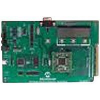
MCP3909EV-MCU16
Description
EVALUATION BOARD FOR MCP3909
Manufacturer
Microchip Technology
Datasheets
1.MCP3909T-ISS.pdf
(44 pages)
2.MCP3909T-ISS.pdf
(104 pages)
3.MCP3909EV-MCU16.pdf
(38 pages)
Specifications of MCP3909EV-MCU16
Number Of Adc's
2
Number Of Bits
16
Sampling Rate (per Second)
15k
Data Interface
Serial
Inputs Per Adc
1 Differential
Input Range
±1 V
Voltage Supply Source
Analog and Digital
Operating Temperature
-40°C ~ 85°C
Utilized Ic / Part
MCP3909
Silicon Manufacturer
Microchip
Application Sub Type
ADC
Kit Application Type
Data Converter
Silicon Core Number
MCP3909
Kit Contents
Board
Lead Free Status / RoHS Status
Lead free / RoHS Compliant


MCP3909
DS22025B-page 4
ELECTRICAL CHARACTERISTICS (CONTINUED)
Electrical Specifications: Unless otherwise indicated, all parameters apply at AV
Internal V
ADC/PGA Specifications
Offset Error
Gain Error Match
Internal Voltage Reference
Voltage
Tolerance
Tempco
Reference Input
Input Range
Input Impedance
Input Capacitance
Analog Inputs
Maximum Signal Level
Differential Input Voltage
Range Channel 0
Differential Input Voltage
Range Channel 1
Input Impedance
Oscillator Input
Frequency Range
Power Specifications
Operating Voltage
I
I
Note 1:
DD,A
DD,D
2:
3:
4:
5:
6:
7:
Parameter
REF
Measurement error = (Energy Measured By Device - True Energy)/True Energy * 100%. Accuracy is
measured with signal (±660 mV) on Channel 1. F
See typical performance curves for higher frequencies and increased dynamic range. This parameter is
not 100% production tested.
Does not include internal V
measured output frequency and expected transfer function.
Percent of HF
CH2 = 100 mV
Error applies down to 60 degree lead (PF = 0.5 capacitive) and 60 degree lag (PF = 0.5 inductive).
Refer to Section 4.0 “Device Overview” for complete description.
Specified by characterization, not production tested.
1 MCLK period at 3.58 MHz is equivalent to less than < 0.005 degrees at 50 or 60 Hz.
, HPF turned on (AC mode), A
OUT
RMS
output frequency variation; Includes external V
@ 50 Hz, AV
MCLK
I
Sym
I
V
DD,D
DD,A
OS
REF
. Gain = 1, CH0 = 470 mVDC, CH1 = 660 mVDC, difference between
GND
DD
Min
390
2.2
3.2
4.5
—
—
—
—
—
—
—
—
—
—
—
1
= 5V + 1 V
, D
GND
Typ.
0.5
2.4
2.3
0.8
±2
15
—
—
—
—
—
—
—
—
—
2
= 0V, MCLK = 3.58 MHz; T
pp
OUT0
@ 100 Hz. DC PSRR: 5V ±500 mV
±470/G
±660
Max
2.6
5.5
2.8
1.2
—
—
—
10
±1
—
—
—
5
4
, F
OUT1
% F
ppm/°C
Units
MHz
pulse outputs. Valid from 45 Hz to 75 Hz.
mV
mV
mV
mA
mA
kΩ
kΩ
pF
%
V
V
V
V
OUT
REF
= 2.5V, CH1 = 100 mV
Referred to Input, applies to both
channels
(Note 5)
CH0+,CH0-,CH1+,CH1- to A
G = PGA Gain on Channel 0
Proportional to 1/MCLK
AV
AV
DV
A
DD
= -40°C to +85°C.
DD,
DD
DD
= DV
© 2009 Microchip Technology Inc.
pin only
pin only
DV
DD
DD
= 4.5V to 5.5V,
Comment
RMS
@ 50 Hz,
GND
Related parts for MCP3909EV-MCU16
Image
Part Number
Description
Manufacturer
Datasheet
Request
R

Part Number:
Description:
Manufacturer:
Microchip Technology Inc.
Datasheet:
Part Number:
Description:
Manufacturer:
Microchip Technology Inc.
Datasheet:
Part Number:
Description:
Manufacturer:
Microchip Technology Inc.
Datasheet:
Part Number:
Description:
Manufacturer:
Microchip Technology Inc.
Datasheet:
Part Number:
Description:
Manufacturer:
Microchip Technology Inc.
Datasheet:
Part Number:
Description:
Manufacturer:
Microchip Technology Inc.
Datasheet:
Part Number:
Description:
Manufacturer:
Microchip Technology Inc.
Datasheet:
Part Number:
Description:
Manufacturer:
Microchip Technology Inc.
Datasheet: