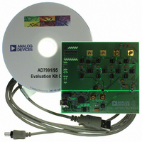
EVAL-AD7991EBZ Analog Devices Inc, EVAL-AD7991EBZ Datasheet - Page 21
EVAL-AD7991EBZ
Manufacturer Part Number
EVAL-AD7991EBZ
Description
BOARD EVAL FOR AD7991
Manufacturer
Analog Devices Inc
Specifications of EVAL-AD7991EBZ
Number Of Adc's
1
Number Of Bits
12
Sampling Rate (per Second)
1M
Data Interface
Serial
Inputs Per Adc
4 Single Ended
Input Range
0 ~ Vdd
Power (typ) @ Conditions
4.4mW @ 5.5 V, 3.4MHz
Voltage Supply Source
Single Supply
Operating Temperature
-40°C ~ 125°C
Utilized Ic / Part
AD7991
Silicon Manufacturer
Analog Devices
Application Sub Type
ADC
Kit Application Type
Data Converter
Silicon Core Number
AD7991
Kit Contents
Board
Rohs Compliant
Yes
Lead Free Status / RoHS Status
Lead free / RoHS Compliant


SAMPLE DELAY AND BIT TRIAL DELAY
It is recommended that no I
conversion is taking place (see Figure 27 and the Placing the
AD7991/AD7995/AD7999 into High Speed Mode section).
However, if this is not always possible, then in order to maintain
the performance of the ADC, Bits D0 and D1 in the configuration
register are used to delay critical sample intervals and bit trials
from occurring while there is activity on the I
a quiet period for each bit decision. However, the sample delay
protection may introduce excessive jitter, degrading the SNR for
large signals above 300 Hz. For guaranteed ac performance, use
of clock stretching is recommended.
When Bit D0 and Bit D1 are both 0, the bit trial and sample interval
delay mechanism is implemented. The default setting of D0 and D1
is 0. To turn off both delay mechanisms, set D0 and D1 to 1.
Table 12. Conversion Value Register (First Read)
D15
Leading 0
Table 13. Conversion Value Register (Second Read)
D7
B7
D14
Leading 0
D6
B6
2
C bus activity occur while a
D13
CH
D5
B5
ID1
2
C bus. This results in
D12
CH
D4
B4
ID0
Rev. B | Page 21 of 28
D11
MSB
D3
B3/0
CONVERSION RESULT REGISTER
The conversion result register is a 16-bit read-only register that
stores the conversion result from the ADC in straight binary
format. A 2-byte read is necessary to read data from this
register. Table 12 shows the contents of the first byte to be read
from AD7991/AD7995/AD7999, and Table 13 shows the
contents of the second byte to be read.
Each AD7991/AD7995/AD7999 conversion result consists of
two leading 0s, two channel identifier bits, and the 12-/10-/8-bit
data result. For the AD7995, the two LSBs (D1 and D0) of the
second read contain two trailing 0s. For the AD7999, the four
LSBs (D3, D2, D1, and D0) of the second read contain four
trailing 0s.
D10
B10
D2
B2/0
AD7991/AD7995/AD7999
D9
B9
D1
B1/0
D8
B8
D0
B0/0
Related parts for EVAL-AD7991EBZ
Image
Part Number
Description
Manufacturer
Datasheet
Request
R


Part Number:
Description:
BOARD EVAL FOR SI270X-A
Manufacturer:
Silicon Laboratories Inc
Datasheet:

Part Number:
Description:
BUCK CONV REF DESIGN KIT IP1201
Manufacturer:
International Rectifier
Datasheet:
Part Number:
Description:
BOARD DEMO SYNC DUAL BUCK CNVTER
Manufacturer:
International Rectifier
Datasheet:
Part Number:
Description:
BOARD DEMO SYNC BUCK CONVETER
Manufacturer:
International Rectifier
Datasheet:

Part Number:
Description:
EVALBOARD/EB Omnidirectional microphone - Analog
Manufacturer:
Analog Devices
Datasheet:
Part Number:
Description:
EVALBOARD/EB Omnidirectional microphone - Analog
Manufacturer:
Analog Devices
Datasheet:


Part Number:
Description:
BOARD EVAL LED DRIVER LT3756
Manufacturer:
Linear Technology
Datasheet:

Part Number:
Description:
BOARD EVAL FOR AD7741/7742
Manufacturer:
Analog Devices Inc
Datasheet:

Part Number:
Description:
±1.7g Dual-Axis IMEMS Accelerometer Evaluation Board
Manufacturer:
Analog Devices Inc
Datasheet:

Part Number:
Description:
IC MULTIPLIER ANALOG 8-SOIC T/R
Manufacturer:
Analog Devices Inc
Datasheet:

Part Number:
Description:
IC ANALOG MULTIPLIER 8-DIP
Manufacturer:
Analog Devices Inc
Datasheet:
Part Number:
Description:
IC ANALOG MULTIPLIER 8-SOIC
Manufacturer:
Analog Devices Inc
Datasheet:
Part Number:
Description:
IC ANALOG MULTIPLIER 8-DIP
Manufacturer:
Analog Devices Inc
Datasheet: