CDB5571 Cirrus Logic Inc, CDB5571 Datasheet - Page 32
CDB5571
Manufacturer Part Number
CDB5571
Description
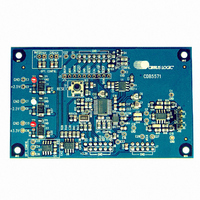
DEV BOARD FOR CS5571 W/MUX
Manufacturer
Cirrus Logic Inc
Type
A/Dr
Specifications of CDB5571
Number Of Adc's
1
Number Of Bits
16
Sampling Rate (per Second)
100k
Data Interface
Serial
Inputs Per Adc
2 Single
Input Range
2.4 ~ 4.2 V
Voltage Supply Source
Dual ±
Operating Temperature
-40°C ~ 85°C
Utilized Ic / Part
CS5571
Product
Data Conversion Development Tools
Conversion Rate
100 KSPS
Resolution
16 bit
Maximum Clock Frequency
16 MHz
Interface Type
SPI
Supply Voltage (max)
3.3 V
Supply Voltage (min)
- 2.5 V
For Use With/related Products
CS5571
Lead Free Status / RoHS Status
Contains lead / RoHS non-compliant
Lead Free Status / RoHS Status
Lead free / RoHS Compliant, Contains lead / RoHS non-compliant
Other names
598-1275
CDB5571-1
CDB5571-1


3/25/08
CS5571
10:56
SCLK – Serial Clock Input/Output, Pin 23
The SMODE pin determines whether the SCLK signal is an input or an output signal. SCLK
determines the rate at which data is clocked out of the SDO pin. If the converter is in SSC
mode, the SCLK frequency will be determined by the master clock frequency of the converter
(either MCLK or the internal oscillator). In SEC mode, the user determines the SCLK frequency.
If SCLK is an output (SMODE = VL), it will be in a high-impedance state when CS is high.
RDY – Ready, Pin 24
If CONV is low the converter will immediately start a conversion and RDY will remain high until
the conversion is completed. At the end of any conversion RDY falls to indicate that a conver-
sion word has been placed into the serial port. RDY will return high after all data bits are shifted
out of the serial port or two master clock cycles before new data becomes available if the CS pin
is inactive (high); or two master clock cycles before new data becomes available if the user
holds CS low but has not started reading the data from the converter when in SEC mode.
32
DS768PP1
Related parts for CDB5571
Image
Part Number
Description
Manufacturer
Datasheet
Request
R

Part Number:
Description:
Development Kit
Manufacturer:
Cirrus Logic Inc
Datasheet:
Part Number:
Description:
Development Kit
Manufacturer:
Cirrus Logic Inc
Datasheet:


Part Number:
Description:
High-efficiency PFC + Fluorescent Lamp Driver Reference Design
Manufacturer:
Cirrus Logic Inc
Datasheet:
Part Number:
Description:
Development Kit
Manufacturer:
Cirrus Logic Inc
Datasheet:
Part Number:
Description:
Development Kit
Manufacturer:
Cirrus Logic Inc
Datasheet:

Part Number:
Description:
Development Kit
Manufacturer:
Cirrus Logic Inc
Datasheet:
Part Number:
Description:
Development Kit
Manufacturer:
Cirrus Logic Inc
Datasheet:
Part Number:
Description:
Development Kit
Manufacturer:
Cirrus Logic Inc
Datasheet:
Part Number:
Description:
Development Kit
Manufacturer:
Cirrus Logic Inc
Datasheet:

Part Number:
Description:
EVALUATION BOARD FOR CS8427
Manufacturer:
Cirrus Logic Inc
Datasheet:

Part Number:
Description:
BOARD EVAL FOR CS8416 RCVR
Manufacturer:
Cirrus Logic Inc
Datasheet:

Part Number:
Description:
EVALUATION BOARD FOR CS8420
Manufacturer:
Cirrus Logic Inc
Datasheet:

Part Number:
Description:
KIT DEVELOPMENT EP9315 ARM9
Manufacturer:
Cirrus Logic Inc
Datasheet:

Part Number:
Description:
KIT DEVELOPMENT EP9302 ARM9
Manufacturer:
Cirrus Logic Inc
Datasheet: