CDB5368 Cirrus Logic Inc, CDB5368 Datasheet - Page 23
CDB5368
Manufacturer Part Number
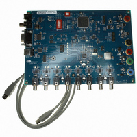
CDB5368
Description
BOARD EVAL FOR CS5368 192KHZ ADC
Manufacturer
Cirrus Logic Inc
Specifications of CDB5368
Number Of Adc's
1
Number Of Bits
24
Sampling Rate (per Second)
192k
Data Interface
Serial
Inputs Per Adc
8 Differential
Input Range
±0.3 V
Voltage Supply Source
Analog and Digital
Operating Temperature
-40°C ~ 85°C
Utilized Ic / Part
CS5368
Description/function
Audio A/D
Operating Supply Voltage
3.3 V
Product
Audio Modules
For Use With/related Products
CS5368
Lead Free Status / RoHS Status
Contains lead / RoHS non-compliant
Lead Free Status / RoHS Status
Lead free / RoHS Compliant, Contains lead / RoHS non-compliant
Other names
598-1157


DS624F4
4.5.2 TDM Format
4.5.3 Configuring Serial Audio Interface Format
4.6
4.6.1 Sample Rate Ranges
4.6.2 Using M1 and M0 to Set Sampling Parameters
T D M O U T
S C L K
F S
Speed Modes
In TDM Mode, all eight channels of audio data are serially clocked out during a single Frame Sync (FS)
cycle, as shown in
channel slot occupies 32 SCLK cycles, with the data left justified and with MSB first. TDM output data
should be latched on the rising edge of SCLK within time specified under
ing” section on page
complimentary TDM data. All SDOUT pins will remain active during TDM Mode. Refer to
timizing Performance in TDM Mode” on page 29
The serial audio interface format of the data is controlled by the configuration of the DIF1 and DIF0 pins in
Stand-Alone Mode or by the DIF[1] and DIF[0] bits in the Global Mode Control Register in Control Port
Mode, as shown in
CS5368 supports sampling rates from 2 kHz to 21 kHz, divided into three ranges: 2 kHz - 54 kHz, 54 kHz -
108 kHz, and 108 kHz - 216 kHz. These sampling speed modes are called Single-Speed Mode (SSM),
Double-Speed Mode (DSM), and Quad-Speed Mode (QSM), respectively.
The Master/Slave operation and the sample rate range are controlled through the settings of the M1 and
M0 pins in Stand-Alone Mode, or by the M[1] and M[0] bits in the Global Mode Control Register in Control
Port Mode, as shown in
M S B
L S B
M1
0
0
1
1
M S B
D a t a
C h a n n e l 1
3 2 c lk s
L S B
L S B
M0
0
1
0
1
Z e r o e s
DIF1
M S B
0
0
1
1
Table
Figure
C h a n n e l 2
16. The TDM data output port resides on the SDOUT1 pin. The TDM output pin is
3 2 c lk s
Table
DIF0
2.
L S B
12. The rising edge of FS signifies the start of a new TDM frame cycle. Each
Quadruple-Speed Master Mode (QSM)
0
1
0
1
Double-Speed Master Mode (DSM)
Single-Speed Master Mode (SSM)
Auto-Detected Speed Slave Mode
M S B
3.
Table 2. DIF1 and DIF0 Pin Settings
C h a n n e l 3
3 2 c lk s
Table 3. M1 and M0 Settings
Figure 12. TDM Format
L S B
M S B
Mode
C h a n n e l 4
3 2 c lk s
for critical system design information.
L S B
Left-Justified
Reserved
M S B
Mode
TDM
C h a n n e l 5
I²S
3 2 c lk s
L S B
M S B
C h a n n e l 6
3 2 c lk s
‘Serial Audio Interface - TDM Tim-
L S B
M S B
C h a n n e l 7
3 2 c lk s
Frequency Range
108 kHz - 216 kHz
54 kHz - 108 kHz
2 kHz - 216 kHz
2 kHz - 54 kHz
L S B
M S B
Section 4.11 “Op-
C h a n n e l 8
3 2 c lk s
CS5368
L S B
M S B
23
Related parts for CDB5368
Image
Part Number
Description
Manufacturer
Datasheet
Request
R

Part Number:
Description:
Development Kit
Manufacturer:
Cirrus Logic Inc
Datasheet:
Part Number:
Description:
Development Kit
Manufacturer:
Cirrus Logic Inc
Datasheet:


Part Number:
Description:
High-efficiency PFC + Fluorescent Lamp Driver Reference Design
Manufacturer:
Cirrus Logic Inc
Datasheet:
Part Number:
Description:
Development Kit
Manufacturer:
Cirrus Logic Inc
Datasheet:
Part Number:
Description:
Development Kit
Manufacturer:
Cirrus Logic Inc
Datasheet:

Part Number:
Description:
Development Kit
Manufacturer:
Cirrus Logic Inc
Datasheet:
Part Number:
Description:
Development Kit
Manufacturer:
Cirrus Logic Inc
Datasheet:
Part Number:
Description:
Development Kit
Manufacturer:
Cirrus Logic Inc
Datasheet:
Part Number:
Description:
Development Kit
Manufacturer:
Cirrus Logic Inc
Datasheet:

Part Number:
Description:
EVALUATION BOARD FOR CS8427
Manufacturer:
Cirrus Logic Inc
Datasheet:

Part Number:
Description:
BOARD EVAL FOR CS8416 RCVR
Manufacturer:
Cirrus Logic Inc
Datasheet:

Part Number:
Description:
EVALUATION BOARD FOR CS8420
Manufacturer:
Cirrus Logic Inc
Datasheet:

Part Number:
Description:
KIT DEVELOPMENT EP9315 ARM9
Manufacturer:
Cirrus Logic Inc
Datasheet:

Part Number:
Description:
KIT DEVELOPMENT EP9302 ARM9
Manufacturer:
Cirrus Logic Inc
Datasheet: