CDB5529 Cirrus Logic Inc, CDB5529 Datasheet
CDB5529
Specifications of CDB5529


Related parts for CDB5529


CDB5529 Summary of contents
Page 1
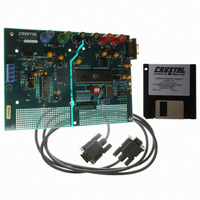
... P.O. Box 17847, Austin, Texas 78760 (512) 445 7222 FAX: (512) 445 7581 http://www.crystal.com General Description The CDB5529 is an inexpensive tool designed to evalu- ate the performance of the CS5529 16-bit Analog-to- Digital Converter (ADC). The evaluation board includes an LT1019 voltage refer- ...
Page 2
... It contains the microcontroller, a Motorola MC145407 interface chip, and test switches. The test switches aid in debugging communication problems between the CDB5529 and the PC. The microcontroller derives its clock from an 11.0592 MHz crystal. From this, the controller is configured to communicate via RS-232 at 9600 baud, no pari- ty, 8-bit data, and 1 stop bit ...
Page 3
... SDI C4 SDO 0.68µF SCLK 1, AIN- 4 AIN AGND HDR2 HDR5 20 1,LT1019 REF+ 2,REF+ 3,REF- 19 4,VA- REF- DGND VA- XOUT XIN 10 11 C15 0.1µF Y2 32768Hz Figure 1. Analog Schematic Section CDB5529 HDR3 13 +5V / 3.3V Digital C11 C31 0.1µF 10µF HDR9 Figure 2 HDR6 3 ...
Page 4
Digital P1.0 VDD 200 P0 SDI P1.1 200 R3 3 SDO P1.2 200 P3 SCLK P1.3 P3.1 From 200 Figure P1.4 200 P3 P1.5 P3.3 ...
Page 5
... Hz output word rates can be attained when a 100kHz clock source is used. Since the CS5529 has such a high degree of integration and flexibility, the CS5529 data sheet should be read thoroughly before and consulted during the use of the CDB5529. To HDR3 C6 C20 R21 47µF 0.1µ ...
Page 6
... IBM, AT and PS/2 are trademarks of International Busi- ness Machines Corporation. Windows is a trademark of Microsoft Corporation. Lab Windows and CVI are trademarks of National Instruments. SPI is a trademark of Motorola. MICROWIRE is a trademark of National Semiconduc- tor. CDB5529 DS246DB1 ...
Page 7
... OK and the Run-Time Engine be installed there. 8) After the Run-Time Engine user is prompted to enter the directory in which to install the CDB5529 software. Select OK to accept the default directory. 9) The program takes a few minutes to install. After the program is installed, double click on the Eval5529 icon to launch it. After a few seconds, the user should be in the graphical user interface environment ...
Page 8
... The following are controls and indicators as- sociated with this window. Acquire: This is a control icon. When pressed, the PC transmits the collect single conversion command CDB5529 DS246DB1 ...
Page 9
... STOP: Stops the collection of conversion data. Write All Registers: This is a control icon. When pressed, the 72 binary input icons settings are ac- quired. This data is then transmitted to the ADC’s gain, offset, and configuration registers. Then, the PC’s display is updated to reflect the registers changes. CDB5529 9 ...
Page 10
... Then click on the graph again to select the second point (the 2nd point is the bottom right corner of the zoom box). Once an area has been zoomed in to, the OUTPUT functions CDB5529 DS246DB1 ...
Page 11
... MAXIMUM: Indicator for the maximum value of the collected data set. MINIMUM: Indicator for the minimum value of the collected data set. OUTPUT: See description in Histogram Window Overview. TEST: See description in Histogram Window Overview. ZOOM: See description in Histogram Window Overview. CDB5529 11 ...
Page 12
... If the mode passes, the LED’s toggle. Note: Remember, to return to the normal operating mode, set the test switches to binary zero, return HDR7 to Normal, and reset the evaluation board. CDB5529 From there, user DS246DB1 ...
Page 13
... DS246DB1 Figure 4. Main Menu Figure 5. Input/Output Window CDB5529 13 ...
Page 14
... Figure 6. Frequency Domain Analysis Figure 7. Configuration Menu CDB5529 DS246DB1 ...
Page 15
... DS246DB1 Figure 8. Time Domain Analysis Figure 9. Histogram Analysis CDB5529 15 ...
Page 16
... Figure 10. CDB5529 Component Side Silkscreen CDB5529 DS246DB1 ...
Page 17
... DS246DB1 Figure 11. CDB5529 Component Side (top) CDB5529 17 ...
Page 18
... Figure 12. CDB5529 Solder Side (bottom) CDB5529 DS246DB1 ...
Page 19
Notes • ...
Page 20
...