KDC2708CEVAL Intersil, KDC2708CEVAL Datasheet - Page 2
KDC2708CEVAL
Manufacturer Part Number
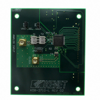
KDC2708CEVAL
Description
DAUGHTER CARD FOR KAD2708
Manufacturer
Intersil
Series
FemtoCharge™r
Datasheets
1.KAD2708C-10Q68.pdf
(16 pages)
2.KMB-001LEVALZ.pdf
(7 pages)
3.KDC5514EVALZ.pdf
(9 pages)
Specifications of KDC2708CEVAL
Number Of Adc's
1
Number Of Bits
8
Sampling Rate (per Second)
275M
Data Interface
Parallel
Inputs Per Adc
1 Differential
Input Range
1.5 Vpp
Power (typ) @ Conditions
261mW @ 275MSPS
Voltage Supply Source
Single Supply
Operating Temperature
-40°C ~ 85°C
Utilized Ic / Part
KAD2708C-27, KMB001 Motherboard
For Use With
KMB001LEVAL - MOTHERBOARD FOR LVDS ADC CARD
Lead Free Status / RoHS Status
Lead free / RoHS Compliant


Table of Contents
Absolute Maximum Ratings ........................................ 3
Thermal Information ..................................................... 3
Electrical Specifications .............................................. 3
Digital Specifications ................................................... 4
Timing Diagram ............................................................ 6
Timing Specifications .................................................. 6
ESD ................................................................................ 6
Pin Descriptions ........................................................... 7
Pin Configuration ......................................................... 8
Typical Performance Curves ....................................... 9
Functional Description ................................................ 12
Equivalent Circuits ....................................................... 14
Layout Considerations ................................................ 15
Definitions ..................................................................... 15
Package Outline Drawing ............................................ 16
Reset ......................................................................... . 12
Voltage Reference ..................................................... . 12
Analog Input .............................................................. . 12
Clock Input ................................................................. . 13
Jitter ........................................................................... . 13
Digital Outputs ........................................................... . 14
Split Ground and Power Planes ................................ . 15
Clock Input Considerations ........................................ . 15
Bypass and Filtering .................................................. . 15
LVCMOS Outputs ...................................................... . 15
Unused Inputs ........................................................... . 15
2
KAD2708C
April 14, 2011
FN6812.1
Related parts for KDC2708CEVAL
Image
Part Number
Description
Manufacturer
Datasheet
Request
R

Part Number:
Description:
Intersil Corporation [CMOS Serial Controller Interface]
Manufacturer:
Intersil Corporation
Datasheet:
Part Number:
Description:
Manufacturer:
Intersil Corporation
Datasheet:
Part Number:
Description:
357-036-542-201 CARDEDGE 36POS DL .156 BLK LOPRO
Manufacturer:
Intersil Corporation
Datasheet:
Part Number:
Description:
1024-Word x 4-Bit LSI Static RAM
Manufacturer:
Intersil Corporation
Datasheet:
Part Number:
Description:
General Purpose NPN Transistor Arrays FN341.4
Manufacturer:
Intersil Corporation
Datasheet:
Part Number:
Description:
CMOS 16-Bit Microprocessor
Manufacturer:
Intersil Corporation
Datasheet:
Part Number:
Description:
Manufacturer:
Intersil Corporation
Datasheet:
Part Number:
Description:
Manufacturer:
Intersil Corporation
Datasheet:
Part Number:
Description:
Manufacturer:
Intersil Corporation
Datasheet:
Part Number:
Description:
Manufacturer:
Intersil Corporation
Datasheet:
Part Number:
Description:
CMOS 6-Bit Latch and Decoder Memory Interfaces
Manufacturer:
Intersil Corporation
Datasheet:
Part Number:
Description:
CA3046General Purpose NPN Transistor Arrays
Manufacturer:
Intersil Corporation
Datasheet:
Part Number:
Description:
Manufacturer:
Intersil Corporation
Datasheet:
Part Number:
Description:
TR909 DLC/FLC SLIC with Low Power Standby
Manufacturer:
Intersil Corporation
Datasheet:
Part Number:
Description:
Manufacturer:
Intersil Corporation
Datasheet: