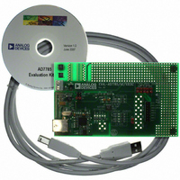
EVAL-AD7785EBZ Analog Devices Inc, EVAL-AD7785EBZ Datasheet - Page 18

EVAL-AD7785EBZ
Manufacturer Part Number
EVAL-AD7785EBZ
Description
BOARD EVALUATION FOR AD7785
Manufacturer
Analog Devices Inc
Specifications of EVAL-AD7785EBZ
Number Of Adc's
1
Number Of Bits
20
Sampling Rate (per Second)
470
Data Interface
Serial
Inputs Per Adc
3 Differential
Input Range
±VREF
Voltage Supply Source
Analog and Digital
Operating Temperature
-40°C ~ 105°C
Utilized Ic / Part
AD7785
Lead Free Status / RoHS Status
Lead free / RoHS Compliant
AD7785
Bit Location
CON7
CON6 to
CON5
CON4
CON3
CON2 to
CON0
DATA REGISTER
RS2, RS1, RS0 = 0, 1, 1; Power-On/Reset = 0x00000F
The conversion result from the ADC is stored in this data register. This is a read-only register. On completion of a read operation from
this register, the RDY bit/pin is set. This is a 24-bit register. The 20-bit conversion is contained in the 20 MSBs. The 4 LSBs are set to 1.
ID REGISTER
RS2, RS1, RS0 = 1, 0, 0; Power-On/Reset = 0xXB
The identification number for the AD7785 is stored in the ID register. This is a read-only register.
IO REGISTER
RS2, RS1, RS0 = 1, 0, 1; Power-On/Reset = 0x00
The IO register is an 8-bit register from which data can be read or to which data can be written. This register is used to enable and select
the value of the excitation currents. Table 16 outlines the bit designations for the IO register. IO0 through IO7 indicate the bit locations;
IO denotes that the bits are in the IO register. IO7 denotes the first bit of the data stream. The number in parentheses indicates the power-
on/reset default status of that bit.
IO7
0(0)
IO6
0(0)
Bit Name
REFSEL
0
BUF
0
CH2 to
CH0
IO5
0(0)
Description
Reference Select Bit. The reference source for the ADC is selected using this bit.
REFSEL
0
1
These bits must be programmed with a Logic 0 for correct operation.
Configures the ADC for buffered or unbuffered mode of operation. If cleared, the ADC operates in unbuffered
mode, lowering the power consumption of the device. If set, the ADC operates in buffered mode, allowing the
user to place source impedances on the front end without contributing gain errors to the system. The buffer
can be disabled when the gain equals 1 or 2. For higher gains, the buffer is automatically enabled.
With the buffer disabled, the voltage on the analog input pins can be from 30 mV below GND to 30 mV above
AV
to 100 mV within the power supply rails.
This bit must be programmed with a Logic 0 for correct operation.
Channel Select Bits. Written by the user to select the active analog input channel to the ADC.
CH2
0
0
0
0
1
1
1
1
DD
IO4
0(0)
. When the buffer is enabled, it requires some headroom, so the voltage on any input pin must be limited
CH1
0
0
1
1
0
0
1
1
Reference Source
External Reference Applied between REFIN(+) and REFIN(–).
Internal Reference Selected.
IO3
IEXCDIR1(0)
0
CH0
0
1
0
1
0
1
1
Channel
AIN1(+) – AIN1(–)
AIN2(+) – AIN2(–)
AIN3(+) – AIN3(–)
AIN1(−) – AIN1(−)
Reserved
Reserved
Temp Sensor
AV
Rev. 0 | Page 18 of 32
DD
Monitor
IO2
IEXCDIR0(0)
Calibration Pair
0
1
2
0
Automatically selects gain = 1 and internal reference
Automatically selects gain = 1/6 and 1.17 V
reference
IO1
IEXCEN1(0)
IO0
IEXCEN0(0)


