EVAL-AD7678CB Analog Devices Inc, EVAL-AD7678CB Datasheet - Page 15
EVAL-AD7678CB
Manufacturer Part Number
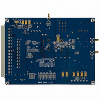
EVAL-AD7678CB
Description
BOARD EVALUATION FOR AD7678
Manufacturer
Analog Devices Inc
Series
PulSAR®r
Specifications of EVAL-AD7678CB
Number Of Adc's
1
Number Of Bits
18
Sampling Rate (per Second)
100k
Data Interface
Serial, Parallel
Inputs Per Adc
1 Differential
Input Range
±VREF
Power (typ) @ Conditions
31mW @ 100kSPS
Voltage Supply Source
Analog and Digital
Operating Temperature
-40°C ~ 85°C
Utilized Ic / Part
AD7678
Lead Free Status / RoHS Status
Contains lead / RoHS non-compliant


CIRCUIT INFORMATION
The AD7678 is a very fast, low power, single-supply, precise
18-bit analog-to-digital converter (ADC) using successive
approximation architecture.
The AD7678’s linearity and dynamic range are similar or better
than many - ADCs. With the advantages of its successive
architecture, which ease multiplexing and reduce power with
throughput, it can be advantageous in applications that
normally use - ADCs.
The AD7678 provides the user with an on-chip track/hold,
successive approximation ADC that does not exhibit any
pipeline or latency, making it ideal for multiple multiplexed
channel applications.
The AD7678 can be operated from a single 5 V supply and can
be interfaced to either 5 V or 3 V digital logic. It is housed in a
48-lead LQFP, or a tiny 48-lead LFCSP package that offers space
savings and allows for flexible configurations as either a serial
or parallel interface. The AD7678 is pin-to-pin compatible with
the AD7674, AD7676, and AD7679.
REFGND
REF
IN–
IN+
262,144C 131,072C
262,144C 131,072C
MSB
MSB
Figure 19. ADC Simplified Schematic
Rev. A | Page 15 of 28
4C
4C
2C
2C
CONVERTER OPERATION
The AD7678 is a successive approximation ADC based on a
charge redistribution DAC. Figure 19 shows the simplified
schematic of the ADC. The capacitive DAC consists of two
identical arrays of 18 binary weighted capacitors, which are
connected to the two comparator inputs.
During the acquisition phase, terminals of the array tied to the
comparator’s input are connected to AGND via SW+ and SW–.
All independent switches are connected to the analog inputs.
Thus, the capacitor arrays are used as sampling capacitors and
acquire the analog signal on IN+ and IN– inputs. When the
acquisition phase is complete and the CNVST input goes low, a
conversion phase is initiated. When the conversion phase
begins, SW+ and SW– are opened first. The two capacitor
arrays are then disconnected from the inputs and connected to
the REFGND input. Therefore, the differential voltage between
the IN+ and IN– inputs captured at the end of the acquisition
phase is applied to the comparator inputs, causing the
comparator to become unbalanced. By switching each element
of the capacitor array between REFGND and REF, the
comparator input varies by binary weighted voltage steps
(V
switches, starting with the MSB first, to bring the comparator
back into a balanced condition. After completing this process,
the control logic generates the ADC output code and brings the
BUSY output low.
REF
C
C
/2, V
REF
C
C
/4...V
LSB
LSB
REF
SW+
SW–
COMP
/262144). The control logic toggles these
SWITCHES
CONTROL
CONTROL
LOGIC
CNVST
OUTPUT
03084–0–025
BUSY
CODE
AD7678
Related parts for EVAL-AD7678CB
Image
Part Number
Description
Manufacturer
Datasheet
Request
R

Part Number:
Description:
ENERCHIP CC EVAL KIT
Manufacturer:
Cymbet Corporation
Datasheet:

Part Number:
Description:
BOARD EVAL FOR AD976
Manufacturer:
Analog Devices Inc
Datasheet:

Part Number:
Description:
BOARD EVAL FOR ADXL345
Manufacturer:
Analog Devices Inc
Datasheet:

Part Number:
Description:
ENERCHIP CC SEH EVAL KIT
Manufacturer:
Cymbet Corporation
Datasheet:

Part Number:
Description:
ENERCHIP EP ENERGY HARVEST EVAL
Manufacturer:
Cymbet Corporation
Datasheet:

Part Number:
Description:
EVAL BOARD FOR TW6864-LB2-GR
Manufacturer:
Intersil
Datasheet:
Part Number:
Description:
EVAL BOARD FOR TW8816-LB3-GR
Manufacturer:
Intersil
Datasheet:
Part Number:
Description:
EVAL BOARD FOR TW8817-TA3-GRS
Manufacturer:
Intersil
Datasheet:

Part Number:
Description:
EVALUATION MODULE FOR ADUM4160
Manufacturer:
Analog Devices Inc
Datasheet:

Part Number:
Description:
BOARD EVALUATION ADCMP581BCP
Manufacturer:
Analog Devices Inc
Datasheet:
Part Number:
Description:
BOARD EVALUATION ADM1041
Manufacturer:
Analog Devices Inc
Datasheet:

Part Number:
Description:
EVAL BOARD FOR STM32F107VCT
Manufacturer:
STMicroelectronics
Datasheet:
Part Number:
Description:
BOARD EVAL FOR AD1954
Manufacturer:
Analog Devices Inc
Datasheet:
Part Number:
Description:
BOARD EVAL FOR AD1955
Manufacturer:
Analog Devices Inc
Datasheet:

Part Number:
Description:
BOARD EVAL FOR AD7655
Manufacturer:
Analog Devices Inc
Datasheet: