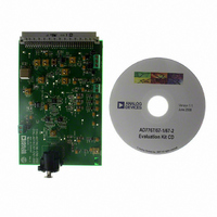
EVAL-AD7767-1EDZ Analog Devices Inc, EVAL-AD7767-1EDZ Datasheet - Page 9
EVAL-AD7767-1EDZ
Manufacturer Part Number
EVAL-AD7767-1EDZ
Description
BOARD EVAL AD7767-1 64KSPS 111DB
Manufacturer
Analog Devices Inc
Specifications of EVAL-AD7767-1EDZ
Number Of Adc's
1
Number Of Bits
24
Sampling Rate (per Second)
64k
Data Interface
Serial
Inputs Per Adc
1 Differential
Input Range
±VREF
Power (typ) @ Conditions
10.5mW @ 64kSPS
Voltage Supply Source
Analog and Digital
Operating Temperature
-40°C ~ 105°C
Utilized Ic / Part
AD7767-1
Lead Free Status / RoHS Status
Lead free / RoHS Compliant


PIN CONFIGURATION AND FUNCTION DESCRIPTIONS
Table 5. Pin Function Descriptions
Pin No.
1
2
3
4
5
6
7
8
9
10
11
12
13
14
15
16
Mnemonic
AV
V
REFGND
V
V
AGND
SYNC/PD
DV
V
SDO
DGND
DRDY
SCLK
MCLK
SDI
CS
REF+
IN+
IN−
DRIVE
DD
DD
Description
+2.5 V Analog Power Supply.
Reference Input for the AD7767. An external reference must be applied to this input pin. The V
from 2.4 V to 5 V. The reference voltage input is independent of the voltage magnitude applied to the AV
Reference Ground. Ground connection for the reference voltage. The input reference voltage (V
decoupled to this pin.
Positive Input of the Differential Analog Input.
Negative Input of the Differential Analog Input.
Power Supply Ground for Analog Circuitry.
Synchronization and Power-Down Input Pin. This pin has dual functionality. It can be used to synchronize multiple
AD7767 devices and/or to put the AD7767 device into power-down mode. See the Power-Down, Reset, and
Synchronization section for further details.
2.5 V Digital Power Supply Input. In cases where an logic voltage of 2.5 V is used for interfacing (2.5 V applied to
V
Logic Power Supply Input, 1.8 V to 3.6 V. The voltage supplied at this pin determines the operating voltage of the
digital logic interface.
Serial Data Output. The conversion result from the AD7767 is output on the SDO pin as a 24-bit, twos complement,
MSB first, serial data stream.
Digital Logic Power Supply Ground.
Data Ready Output. A falling edge on the DRDY signal indicates that a new conversion data result is available in the
output register of the AD7767. See the
Serial Clock Input. The SCLK input provides the serial clock for all serial data transfers with the AD7767 device. See
the AD7767 Interface section for further details.
Master Clock Input. The AD7767 sampling frequency is equal to the MCLK frequency.
Serial Data Input. This is the daisy-chain input of the AD7767. See the Daisy Chaining section for further details.
Chip Select Input. The CS input selects the AD7767 device and acts as an enable on the SDO pin. In cases where CS
is used, the MSB of the conversion result is clocked onto the SDO line on the CS falling edge. The CS input allows
multiple AD7767 devices to share the same SDO line. This allows the user to select the appropriate device by
supplying it with a logic low CS signal, which enables the SDO pin of the device concerned. See the
Interface
DRIVE
pin), the DVDD and V
section for further details.
DRIVE
Figure 6. 16-Lead TSSOP Pin Configuration
SYNC/PD
REFGND
AGND
V
pin may be connected to the same voltage supply rail.
AV
DV
REF+
V
V
IN+
IN–
DD
DD
1
3
4
5
6
8
2
7
Rev. C | Page 9 of 24
AD7767 Interface
(Not to Scale)
AD7767-2
AD767-1/
AD7767/
TOP VIEW
16
15
14
13
12
11
10
9
CS
SDI
MCLK
SCLK
DRDY
DGND
SDO
V
DRIVE
section for further details.
REF+
REF+
input can range
) should be
AD7767
AD7767
DD
pin.
Related parts for EVAL-AD7767-1EDZ
Image
Part Number
Description
Manufacturer
Datasheet
Request
R

Part Number:
Description:
IC, ADJ LDO REG, 1.5V TO 5V 250mA MSOP-8
Manufacturer:
Vishay
Datasheet:

Part Number:
Description:
IC, ADJ LDO REG, 1.5V TO 5V 0.6A 8-TSSOP
Manufacturer:
Vishay
Datasheet:
Part Number:
Description:
IC, ADJ LDO REG, 1.5V TO 5V 250mA MSOP-8
Manufacturer:
Vishay
Datasheet:

Part Number:
Description:
IC ADJ LDO REG 1.5V TO 5V 150mA 5-SOT-23
Manufacturer:
Vishay
Datasheet:

Part Number:
Description:
BOARD EVAL AS1324-AD
Manufacturer:
austriamicrosystems
Datasheet:
Part Number:
Description:
IC, ADJ LDO REG, 1.5V TO 5V 0.6A 8-TSSOP
Manufacturer:
Vishay
Datasheet:

Part Number:
Description:
IC, ADJ LDO REG, 1.5V TO 5V, 0.3A, MSOP8
Manufacturer:
Vishay
Datasheet:
Part Number:
Description:
IC, ADJ LDO REG, 1.5V TO 5V, 0.3A, MSOP8
Manufacturer:
Vishay
Datasheet:
Part Number:
Description:
IC, ADJ LDO REG 1.215V TO 5V 0.3A MSOP-8
Manufacturer:
Vishay
Datasheet:
Part Number:
Description:
IC, ADJ LDO REG 1.215V TO 5V 0.3A MSOP-8
Manufacturer:
Vishay
Datasheet:

Part Number:
Description:
±1.7g Dual-Axis IMEMS Accelerometer Evaluation Board
Manufacturer:
Analog Devices Inc
Datasheet:

Part Number:
Description:
IC MULTIPLIER ANALOG 8-SOIC T/R
Manufacturer:
Analog Devices Inc
Datasheet:

Part Number:
Description:
IC ANALOG MULTIPLIER 8-DIP
Manufacturer:
Analog Devices Inc
Datasheet:
Part Number:
Description:
IC ANALOG MULTIPLIER 8-SOIC
Manufacturer:
Analog Devices Inc
Datasheet:
Part Number:
Description:
IC ANALOG MULTIPLIER 8-DIP
Manufacturer:
Analog Devices Inc
Datasheet: