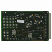
EVAL-AD7725CBZ Analog Devices Inc, EVAL-AD7725CBZ Datasheet - Page 21

EVAL-AD7725CBZ
Manufacturer Part Number
EVAL-AD7725CBZ
Description
BOARD EVALUATION FOR AD7725
Manufacturer
Analog Devices Inc
Datasheet
1.AD7725BSZ.pdf
(28 pages)
Specifications of EVAL-AD7725CBZ
Number Of Adc's
1
Number Of Bits
16
Sampling Rate (per Second)
900k
Data Interface
Serial, Parallel
Inputs Per Adc
1 Differential
Input Range
±VREF
Power (typ) @ Conditions
615mW @ 900kSPS
Voltage Supply Source
Analog and Digital
Operating Temperature
-40°C ~ 85°C
Utilized Ic / Part
AD7725
Lead Free Status / RoHS Status
Lead free / RoHS Compliant
Figures 23 and 24 show plots of filter taps and CLKIN
frequency versus I
To get a more accurate number of taps for a given CLKIN
frequency, see Figure 24.
Figures 23 and 24 were created for a one-stage low-pass FIR
filter, which will give the worst case I
The I
the filter is increased.
MODES OF OPERATION
The AD7725 can operate with either a serial or a parallel interface.
These modes are chosen by setting the logic state of the S/P pin.
REV. A
DD
180
160
140
120
100
Figure 23. Typical I
Numbers of Filter Taps
Figure 24. Typical I
CLKIN Frequencies
80
60
40
20
180
160
140
120
100
0
80
60
40
20
0
will decrease as the amount of decimation employed in
0
0
10
MAXIMUM I
20
MAXIMUM I
2.4
HALF_PWR ENABLED
DD
30
.
DD
40
4.8
DD
DD
DD
FILTER TAPS
50
vs. CLKIN for Various
vs. Filter Taps for Various
CLKIN – MHz
7.2
60
54 TAPS
DD
72 TAPS
70
figures.
9.6
2.4MHz
90 TAPS
HALF_PWR DISABLED
80
90
12.0
1MHz
108 TAPS
14.4MHz
12MHz
9.6MHz
7.2MHz
4.8MHz
36 TAPS
100
110
14.4
–21–
PARALLEL MODE
The parallel mode is selected by tying S/P to DGND. Pro-
gramming the postprocessor and operation of the AD7725 in
parallel mode requires the use of an instruction set. The user
also has access to an on-chip status register that provides infor-
mation about the operation of the device. The parallel interface
is a standard interface that interfaces to digital signal processors
and microprocessors. Figure 25 shows the interface between the
AD7725 and a DSP/microprocessor, and Figures 6, 7, and 8
show the timing of the parallel interface.
Operating the AD7725 in Parallel Mode
The AD7725 uses an instruction set, its interrupt pin output
(the INT pin), and an on-chip status register to communicate
with the DSP/microprocessor. An interrupt is issued by the
AD7725 whenever user intervention is required. The interrupt
can be cleared by either writing an instruction or reading the
status register. At the completion of power-on reset, the
AD7725 will issue an interrupt to indicate that user intervention
is required for it to begin communicating with the DSP/micro-
processor. An instruction should then be issued to load the
configuration data to program the postprocessor. Once the
configuration file has been loaded, another interrupt is issued by
the device. The status register can then be read to check if any
errors occurred during configuration. If no errors occur during
the configuration process, an instruction can be issued to inform
the device to begin converting.
Pins RD/WR, CS, and RS are used along with the data pins D0
to D15 to write instructions/configuration data and read the
status register/conversion data.
During a read cycle, the RS pin informs the AD7725 whether
the status register or a conversion result is being read. When RS
is high, the status register is read while the data register, such as
the device ID or a conversion result, is read when RS is low.
Similarly, during a WR cycle, an instruction is written when RS
is high and data (such as configuration data) is written when RS
is low (see Table I).
RD/WR (Pin 7)
0
0
1
1
Figure 25. AD7725 Parallel Interface to Microprocessor
SYNC
S/P
AD7725
DATA[15:0]
DVAL/INT
RD/WR
Table I. Reading and Writing
CS
RS
RS (Pin 4)
0
1
0
1
DECODER
ADDR
Write Data
Write Instruction
Read Data
Read Status Register
Operation
AD7725
ADDR
WR
RD
DATA[15:0]
INTERRUPT
DSP/ P


