EVAL-AD7731EBZ Analog Devices Inc, EVAL-AD7731EBZ Datasheet - Page 5
EVAL-AD7731EBZ
Manufacturer Part Number
EVAL-AD7731EBZ
Description
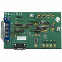
BOARD EVALUATION FOR AD7731
Manufacturer
Analog Devices Inc
Datasheets
1.AD7731BRUZ.pdf
(44 pages)
2.EVAL-AD7731EBZ.pdf
(11 pages)
3.EVAL-AD7731EBZ.pdf
(3 pages)
4.EVAL-AD7731EBZ.pdf
(44 pages)
Specifications of EVAL-AD7731EBZ
Number Of Adc's
1
Number Of Bits
24
Sampling Rate (per Second)
6.4k
Data Interface
Serial
Inputs Per Adc
3 Differential
Input Range
±1.28 V
Power (typ) @ Conditions
67.5mW @ 6.4kSPS
Voltage Supply Source
Analog and Digital
Operating Temperature
-40°C ~ 85°C
Utilized Ic / Part
AD7731
Lead Free Status / RoHS Status
Lead free / RoHS Compliant


ABSOLUTE MAXIMUM RATINGS*
(T
AV
AV
DV
DV
AGND to DGND . . . . . . . . . . . . . . . . . . . . . . –5 V to +0.3 V
AV
Analog Input Voltage to AGND . . . . –0.3 V to AV
Reference Input Voltage to AGND . . –0.3 V to AV
AIN/REF IN Current (Indefinite) . . . . . . . . . . . . . . . . . 30 mA
Digital Input Voltage to DGND . . . . –0.3 V to DV
Digital Output Voltage to DGND . . . –0.3 V to DV
Output Voltage (D0, D1) to DGND . . –0.3 V to AV
Operating Temperature Range
Junction Temperature . . . . . . . . . . . . . . . . . . . . . . . . . +150 C
CAUTION
ESD (electrostatic discharge) sensitive device. Electrostatic charges as high as 4000 V readily
accumulate on the human body and test equipment and can discharge without detection.
Although the AD7731 features proprietary ESD protection circuitry, permanent damage may
occur on devices subjected to high energy electrostatic discharges. Therefore, proper ESD
precautions are recommended to avoid performance degradation or loss of functionality.
REV. 0
A
Industrial (B Version) . . . . . . . . . . . . . . . . –40 C to +85 C
Storage Temperature Range . . . . . . . . . . . –65 C to +150 C
DD
DD
DD
= +25 C unless otherwise noted)
DD
DD
to AGND . . . . . . . . . . . . . . . . . . . . . . . –0.3 V to +7 V
to DGND . . . . . . . . . . . . . . . . . . . . . . . –0.3 V to +7 V
to DV
to AGND . . . . . . . . . . . . . . . . . . . . . . . –0.3 V to +7 V
to DGND . . . . . . . . . . . . . . . . . . . . . . . –0.3 V to +7 V
Model
AD7731BN
AD7731BR
AD7731BRU
EVAL-AD7731EB
DD
. . . . . . . . . . . . . . . . . . . . . . . . . . –2 V to +5 V
Figure 1. Load Circuit for Access Time and Bus Relinquish Time
–40 C to +85 C
–40 C to +85 C
Evaluation Board
Temperature Range
–40 C to +85 C
TO OUTPUT
PIN
50pF
DD
DD
DD
DD
DD
ORDERING GUIDE
+ 0.3 V
+ 0.3 V
+ 0.3 V
+ 0.3 V
+ 0.3 V
Package Description
Plastic DIP
Small Outline
Thin Shrink Small Outline (TSSOP)
–5–
Plastic DIP Package, Power Dissipation . . . . . . . . . . 450 mW
TSSOP Package, Power Dissipation . . . . . . . . . . . . . 450 mW
SOIC Package, Power Dissipation . . . . . . . . . . . . . . . 450 mW
*Stresses above those listed under Absolute Maximum Ratings may cause perma-
nent damage to the device. This is a stress rating only; functional operation of
the device at these or any other conditions above those listed in the operational
sections of this specification is not implied. Exposure to absolute maximum rating
conditions for extended periods may affect device reliability.
I
I
SINK
SOURCE
Lead Temperature (Soldering, 10 sec) . . . . . . . . . . . +260 C
Lead Temperature, Soldering
Lead Temperature, Soldering
JA
JA
JA
Vapor Phase (60 sec) . . . . . . . . . . . . . . . . . . . . . . +215 C
Infrared (15 sec) . . . . . . . . . . . . . . . . . . . . . . . . . . +220 C
Vapor Phase (60 sec) . . . . . . . . . . . . . . . . . . . . . . +215 C
Infrared (15 sec) . . . . . . . . . . . . . . . . . . . . . . . . . . +220 C
(800µA AT DV
100µA AT DV
Thermal Impedance . . . . . . . . . . . . . . . . . . . . . 105 C/W
Thermal Impedance . . . . . . . . . . . . . . . . . . . . . 128 C/W
Thermal Impedance . . . . . . . . . . . . . . . . . . . . . . 75 C/W
(200µA AT DV
100µA AT DV
+1.6V
DD
DD
= +5V
= +3V)
DD
DD
= +3V)
= +5V
WARNING!
Package Options
R-24
RU-24
N-24
ESD SENSITIVE DEVICE
AD7731
Related parts for EVAL-AD7731EBZ
Image
Part Number
Description
Manufacturer
Datasheet
Request
R


Part Number:
Description:
BOARD EVAL FOR SI270X-A
Manufacturer:
Silicon Laboratories Inc
Datasheet:

Part Number:
Description:
BUCK CONV REF DESIGN KIT IP1201
Manufacturer:
International Rectifier
Datasheet:
Part Number:
Description:
BOARD DEMO SYNC DUAL BUCK CNVTER
Manufacturer:
International Rectifier
Datasheet:
Part Number:
Description:
BOARD DEMO SYNC BUCK CONVETER
Manufacturer:
International Rectifier
Datasheet:

Part Number:
Description:
EVALBOARD/EB Omnidirectional microphone - Analog
Manufacturer:
Analog Devices
Datasheet:
Part Number:
Description:
EVALBOARD/EB Omnidirectional microphone - Analog
Manufacturer:
Analog Devices
Datasheet:


Part Number:
Description:
BOARD EVAL LED DRIVER LT3756
Manufacturer:
Linear Technology
Datasheet:

Part Number:
Description:
BOARD EVAL FOR AD7741/7742
Manufacturer:
Analog Devices Inc
Datasheet:

Part Number:
Description:
±1.7g Dual-Axis IMEMS Accelerometer Evaluation Board
Manufacturer:
Analog Devices Inc
Datasheet:

Part Number:
Description:
IC MULTIPLIER ANALOG 8-SOIC T/R
Manufacturer:
Analog Devices Inc
Datasheet:

Part Number:
Description:
IC ANALOG MULTIPLIER 8-DIP
Manufacturer:
Analog Devices Inc
Datasheet:
Part Number:
Description:
IC ANALOG MULTIPLIER 8-SOIC
Manufacturer:
Analog Devices Inc
Datasheet:
Part Number:
Description:
IC ANALOG MULTIPLIER 8-DIP
Manufacturer:
Analog Devices Inc
Datasheet: