CDB5532U Cirrus Logic Inc, CDB5532U Datasheet - Page 43
CDB5532U
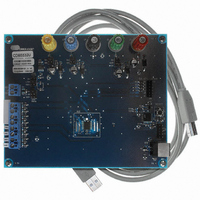
Manufacturer Part Number
CDB5532U
Description
BOARD EVAL FOR CS5532U ADC
Manufacturer
Cirrus Logic Inc
Specifications of CDB5532U
Number Of Adc's
2
Number Of Bits
24
Sampling Rate (per Second)
3.84k
Data Interface
Serial
Inputs Per Adc
1 Differential
Input Range
±2.5 V
Power (typ) @ Conditions
35mW @ 3.84kSPS
Voltage Supply Source
Analog and Digital, Dual ±
Operating Temperature
-40°C ~ 85°C
Utilized Ic / Part
CS5532
Description/function
Audio DSPs
Operating Supply Voltage
5 V
Product
Audio Modules
For Use With/related Products
C8051F320
Lead Free Status / RoHS Status
Contains lead / RoHS non-compliant
Lead Free Status / RoHS Status
Lead free / RoHS Compliant, Contains lead / RoHS non-compliant
Other names
598-1159


2.12. Getting Started
This A/D converter has several features. From a
software programmer’s prospective, what should
be done first? To begin, a 4.9152 MHz or
4.096 MHz crystal takes approximately 20 ms to
start. To accommodate for this, it is recommended
that a software delay of approximately 20 ms start
the processor’s ADC initialization code. Next,
since the CS5532/34 do not provide a power-on-re-
set function, the user must first initialize the ADC
to a known state. This is accomplished by resetting
the ADC’s serial port with the Serial Port Initializa-
tion sequence. This sequence resets the serial port
to the command mode and is accomplished by
transmitting 15 SYNC1 command bytes (0xFF
hexadecimal), followed by one SYNC0 command
(0xFE hexadecimal). Once the serial port of the
ADC is in the command mode, the user must reset
all the internal logic by performing a system reset
sequence (see 2.3.2 System Reset Sequence). The
next action is to initialize the voltage reference
mode. The voltage reference select (VRS) bit in the
DS755F3
configuration register must be set based upon the
magnitude of the reference voltage between the
VREF+ and the VREF- pins.
After this, the channel-setup registers (CSRs) should
be initialized, as these registers determine how cali-
brations and conversions will be performed. Once
the CSRs are initialized, the user has three options in
calibrating the ADC: 1) don’t calibrate and use the
default settings; 2) perform self or system calibra-
tions; or 3) upload previously saved calibration re-
sults to the offset and gain registers. At this point,
the ADC is ready to perform conversions.
2.13. PCB Layout
For optimal performance, the CS5532/34 should be
placed entirely over an analog ground plane. All
grounded pins on the ADC, including the DGND
pin, should be connected to the analog ground
plane that runs beneath the chip. In a split-plane
system, place the analog-digital plane split imme-
diately adjacent to the digital portion of the chip.
CS5532/34-BS
43
Related parts for CDB5532U
Image
Part Number
Description
Manufacturer
Datasheet
Request
R

Part Number:
Description:
Development Kit
Manufacturer:
Cirrus Logic Inc
Datasheet:
Part Number:
Description:
Development Kit
Manufacturer:
Cirrus Logic Inc
Datasheet:


Part Number:
Description:
High-efficiency PFC + Fluorescent Lamp Driver Reference Design
Manufacturer:
Cirrus Logic Inc
Datasheet:
Part Number:
Description:
Development Kit
Manufacturer:
Cirrus Logic Inc
Datasheet:
Part Number:
Description:
Development Kit
Manufacturer:
Cirrus Logic Inc
Datasheet:

Part Number:
Description:
Development Kit
Manufacturer:
Cirrus Logic Inc
Datasheet:
Part Number:
Description:
Development Kit
Manufacturer:
Cirrus Logic Inc
Datasheet:
Part Number:
Description:
Development Kit
Manufacturer:
Cirrus Logic Inc
Datasheet:
Part Number:
Description:
Development Kit
Manufacturer:
Cirrus Logic Inc
Datasheet:

Part Number:
Description:
EVALUATION BOARD FOR CS8427
Manufacturer:
Cirrus Logic Inc
Datasheet:

Part Number:
Description:
BOARD EVAL FOR CS8416 RCVR
Manufacturer:
Cirrus Logic Inc
Datasheet:

Part Number:
Description:
EVALUATION BOARD FOR CS8420
Manufacturer:
Cirrus Logic Inc
Datasheet:

Part Number:
Description:
KIT DEVELOPMENT EP9315 ARM9
Manufacturer:
Cirrus Logic Inc
Datasheet:

Part Number:
Description:
KIT DEVELOPMENT EP9302 ARM9
Manufacturer:
Cirrus Logic Inc
Datasheet: