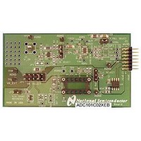
ADC101C02XEB/NOPB National Semiconductor, ADC101C02XEB/NOPB Datasheet - Page 15

ADC101C02XEB/NOPB
Manufacturer Part Number
ADC101C02XEB/NOPB
Description
BOARD EVALUATION FOR ADC101C02X
Manufacturer
National Semiconductor
Specifications of ADC101C02XEB/NOPB
Number Of Adc's
1
Number Of Bits
10
Sampling Rate (per Second)
188.9k
Data Interface
I²C
Inputs Per Adc
1 Single Ended
Power (typ) @ Conditions
780mW @ 22kSPS
Voltage Supply Source
Single Supply
Operating Temperature
-40°C ~ 105°C
Utilized Ic / Part
ADC101C021, ADC101C027
Silicon Manufacturer
National
Silicon Core Number
ADC101C021, ADC101C027
Kit Application Type
Data Converter
Application Sub Type
ADC
Kit Contents
Board
Lead Free Status / RoHS Status
Lead free / RoHS Compliant
Other names
ADC101C02XEB
1.4 REFERENCE VOLTAGE
The ADC101C021 uses the supply (V
V
version will only be as precise as the reference (V
supply voltage should be free of noise. The reference should
be driven by a low output impedance voltage source.
The Applications section provides recommended ways to pro-
vide the supply voltage appropriately. Refer to Section 2.1
TYPICAL APPLICATION CIRCUIT for details.
1.5 POWER-ON RESET
An internal power-on reset (POR) occurs when the supply
voltage transitions above the power-on reset threshold. Each
of the registers contains a defined value upon POR and this
data remains there until any of the following occurs:
•
•
•
The internal registers will lose their contents if the supply volt-
age goes below 2.4V. Should this happen, it is important that
the V
supply is raised again to properly reset the device and ensure
that the ADC performs as specified.
1.6 INTERNAL REGISTERS
The ADC101C021 has 8 internal data registers and one ad-
dress pointer. The registers provide additional ADC functions
such as storing minimum and maximum conversion results,
setting alert threshold levels, and storing data to configure the
operation of the device. Figure 6 shows all of the registers and
their corresponding address pointer values. All of the regis-
ters are read/write capable except the conversion result reg-
ister, which is read-only.
A
must be treated as a reference. The analog-to-digital con-
The first conversion is completed, causing the Conversion
Result and Status registers to be updated.
A different data word is written to a writable register.
The ADC is powered down.
A
supply be lowered to a maximum of 200mV before the
A
) as the reference, so
FIGURE 5. Ideal Transfer Characteristic
A
), so the
15
FIGURE 6. Register Structure
30052068
www.national.com
30052069


