CDB35L00 Cirrus Logic Inc, CDB35L00 Datasheet - Page 7
CDB35L00
Manufacturer Part Number
CDB35L00
Description
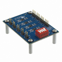
DEVELOPMENT BOARD FOR CS35L0X
Manufacturer
Cirrus Logic Inc
Datasheet
1.CDB35L00.pdf
(12 pages)
Specifications of CDB35L00
Amplifier Type
Class D
Output Type
4-Channel (Quad)
Max Output Power X Channels @ Load
2.7W x 4 @ 4 Ohm
Voltage - Supply
2.5 V ~ 5.5 V
Board Type
Fully Populated
Utilized Ic / Part
CS35L0X
Description/function
Audio Amplifiers
Operating Supply Voltage
2.5 V to 5.5 V
Output Power
1.6 W, 2.7 W
Product
Audio Modules
For Use With/related Products
CS35L00
Lead Free Status / RoHS Status
Contains lead / RoHS non-compliant
Operating Temperature
-
Lead Free Status / Rohs Status
Lead free / RoHS Compliant
Other names
598-1803


DS913DB2
2. GROUNDING AND POWER SUPPLY DECOUPLING
The CS35L00 requires careful attention to power supply and grounding arrangements to optimize performance and
minimize radiated emissions. The device decoupling capacitors should be located as close to the CS35L00 as pos-
sible. This can be optimized by using both top and bottom side component population as demonstrated by the
CDB35L00-X4 board.
2.1
2.2
2.2.1
Power Supply Decoupling
Proper power supply decoupling is one key to maximizing the performance of a Class-D amplifier.
and
the C13, C23, C33, and C43 capacitors connected to the LFILT+ pin. This pin is used as decoupling for the
internal LDO regulator when operating in HD or FHD modes.
The small value decoupling capacitors are placed as close as possible to the power pins of the CS35L00
on the CDB35L00-X4 board. It is recommended that the power supply decoupling capacitors reside on the
opposite side of the board from which the CS35L00 is populated on. This allows for very close placement
of the decoupling capacitors to the power supply pins of the CS35L00 without interfering with the differential
audio inputs or differential audio outputs. This placement keeps the high-frequency current loop small to
minimize EMI.
Electromagnetic Interference (EMI)
This reference design is a board-level solution that is meant to control emissions by minimizing and sup-
pressing them at the source, in contrast to containing them in an enclosure.
Suppression of EMI at the Source
Several techniques are used in the circuit design and board layout to minimize high-frequency fields in
the immediate vicinity of the high-power components. Specific techniques include the following:
• As mentioned in
• Differential input and output signals should be routed differentially whenever possible.
• A solid ground plane on the adjacent PCB layer underneath all high-frequency traces to minimize the
• Optional output EMI filter component landings are available as described in
• Keeping the switching output filter components as close to the amplifier as possible.
Figure 6 on page 11
mizing the loop area of the decoupling loop is one aspect of minimizing EMI.
loop area of the return path.
need to be further reduced.
Section
show the component placement for the CDB35L00-X4 board. Note the addition of
2.1, effective power supply decoupling of high-frequency currents and mini-
Section
CDB35L00-X4
1.7.1, if emissions
Figure 5
7
Related parts for CDB35L00
Image
Part Number
Description
Manufacturer
Datasheet
Request
R

Part Number:
Description:
Audio Modules & Development Tools Eval Bd - DF 4ch ADC 8ch DAC & 32bit DSP
Manufacturer:
Cirrus Logic Inc
Part Number:
Description:
Development Kit
Manufacturer:
Cirrus Logic Inc
Datasheet:
Part Number:
Description:
Development Kit
Manufacturer:
Cirrus Logic Inc
Datasheet:


Part Number:
Description:
High-efficiency PFC + Fluorescent Lamp Driver Reference Design
Manufacturer:
Cirrus Logic Inc
Datasheet:
Part Number:
Description:
Development Kit
Manufacturer:
Cirrus Logic Inc
Datasheet:
Part Number:
Description:
Development Kit
Manufacturer:
Cirrus Logic Inc
Datasheet:

Part Number:
Description:
Development Kit
Manufacturer:
Cirrus Logic Inc
Datasheet:
Part Number:
Description:
Development Kit
Manufacturer:
Cirrus Logic Inc
Datasheet:
Part Number:
Description:
Development Kit
Manufacturer:
Cirrus Logic Inc
Datasheet:

Part Number:
Description:
EVALUATION BOARD FOR CS8427
Manufacturer:
Cirrus Logic Inc
Datasheet:

Part Number:
Description:
BOARD EVAL FOR CS8416 RCVR
Manufacturer:
Cirrus Logic Inc
Datasheet:

Part Number:
Description:
EVALUATION BOARD FOR CS8420
Manufacturer:
Cirrus Logic Inc
Datasheet:

Part Number:
Description:
KIT DEVELOPMENT EP9315 ARM9
Manufacturer:
Cirrus Logic Inc
Datasheet:

Part Number:
Description:
KIT DEVELOPMENT EP9302 ARM9
Manufacturer:
Cirrus Logic Inc
Datasheet: