RDK-115 Power Integrations, RDK-115 Datasheet - Page 11
RDK-115
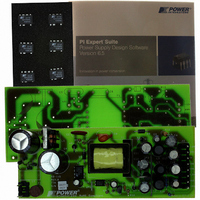
Manufacturer Part Number
RDK-115
Description
KIT REFERENCE DESIGN W/TN376PN
Manufacturer
Power Integrations
Series
TinySwitch®-PKr
Specifications of RDK-115
Main Purpose
AC/DC, Primary Side
Outputs And Type
4, Isolated
Power - Output
7.5W
Voltage - Output
3.3V, 5V, 12V, -12V
Current - Output
500mA, 500mA, 250mA, 30mA
Voltage - Input
85 ~ 265VAC
Regulator Topology
Flyback
Frequency - Switching
132kHz
Board Type
Fully Populated
Utilized Ic / Part
TNY376
Product
Accessories & Kits
Lead Free Status / RoHS Status
Not applicable / Not applicable
Other names
596-1145


Figure 16. Layout Considerations for TinySwitch-PK Using P Package.
Y-Capacitor
The placement of the Y-capacitor should be directly from the
primary input fi lter capacitor positive terminal to the common/
return terminal of the transformer secondary. Such a placement
will route high magnitude common mode surge currents away
from the TinySwitch-PK device. Note – if an input π (C, L, C)
EMI fi lter is used, then the inductor in the fi lter should be placed
between the negative terminals on the input fi lter capacitors.
Optocoupler
Place the optocoupler physically close to the TinySwitch-PK
device to minimize the primary side trace lengths. Keep the
high current, high voltage drain and clamp traces away from the
optocoupler to prevent noise pick up.
Output Diode
For best performance, the area of the loop connecting the
secondary winding, the Output Diode, and the Output Filter
Capacitor should be minimized. In addition, for axial diodes,
suffi cient copper area should be provided at the anode and
cathode terminal of diode for heatsinking. A larger area is
preferred at the quiet cathode terminal. A large anode area can
increase high frequency radiated EMI.
Quick Design Checklist
As with any power supply design, all TinySwitch-PK designs
should be verifi ed on the bench to make sure that component
specifi cations are not exceeded under worst case conditions.
The following minimum set of tests is strongly recommended:
www.powerint.com
TOP VIEW
Copper area for
heat sinking
HV
+
-
Bypass capacitor connection
to device should be short
Input Filter Capacitor
S
S
S
S
C
BP
directly to input capacitor
Return bias winding
EN/UV
D
R
BP
UV
away from drain connected traces
Route connections to EN/UV pin
(including undervoltage resistor)
BIAS
PRI
BIAS
1.
2.
3.
Design Tools
Up-to-date information on design tools can be found at the
Power Integrations web site: www.powerint.com.
PRI
Maximum drain voltage – Verify the V
650 V at highest input voltage and peak (overload) output
power. The 50 V margin to the 700 V BV
gives margin for design variation.
Maximum drain current – At maximum ambient temperature,
maximum input voltage, and peak output (overload) power,
verify drain current waveforms for any signs of transformer
saturation and excessive leading edge current spikes at
startup. Repeat under steady state conditions and verify that
the leading edge current spike event is below I
of the t
current should be below the specifi ed absolute maximum
ratings.
Thermal Check – At specifi ed maximum output power,
minimum input voltage, and maximum ambient temperature,
verify that the temperature specifi cations are not exceeded
for TinySwitch-PK device, transformer, output diode, and
output capacitors. Enough thermal margin should be
allowed for part-to-part variation of the R
TinySwitch-PK device as specifi ed in the data sheet. Under
low-line maximum power, a maximum TinySwitch-PK device
SOURCE pin temperature of 110 °C is recommended to
allow for these variations.
Safety Spacing
Capacitor
coupler
Opto-
Y1-
LEB(Min)
m
T
n
o
a
s
e
r
f
r
r
. Under all conditions the maximum drain
SEC
Maximize hatched copper
areas (
heatsinking
Rectifier
Output
-
TNY375-380
OUT
DC
DS
does not exceed
+
DS(ON)
DSS
) for optimum
specifi cation
of
INIT
at the end
PI-4675-051507
Rev. C 07/09
11
Related parts for RDK-115
Image
Part Number
Description
Manufacturer
Datasheet
Request
R

Part Number:
Description:
KIT REF DESIGN FOR LNK457D
Manufacturer:
Power Integrations
Datasheet:

Part Number:
Description:
REFERENCE DESIGN LINKSWITCH-PH
Manufacturer:
Power Integrations
Datasheet:

Part Number:
Description:
KIT REF DESIGN FOR LNK403EG
Manufacturer:
Power Integrations
Datasheet:

Part Number:
Description:
KIT REF DESIGN FOR LNK406EG
Manufacturer:
Power Integrations
Datasheet:

Part Number:
Description:
KIT REF DESIGN LINKSWITCH-CV
Manufacturer:
Power Integrations
Datasheet:

Part Number:
Description:
KIT REF DESIGN LINKSWITCH 2
Manufacturer:
Power Integrations
Datasheet:

Part Number:
Description:
Specifications: Family: Eval Boards - DC/DC & AC/DC (Off-Line) SMPS ; Series: HiperLCS™ ; Main Purpose: DC/DC, Step Down ; Outputs and Type: 1, Isolated ; Power - Output: 150W ; Voltage - Output: 24V ; Current - Output: 6.25A ; Voltage - Input:
Manufacturer:
Power Integrations, Inc.
Datasheet:

Part Number:
Description:
KIT DESIGN REF TINYSWITCH-III
Manufacturer:
Power Integrations
Datasheet:

Part Number:
Description:
KIT DESIGN REF LINKSWITCH LP
Manufacturer:
Power Integrations
Datasheet:

Part Number:
Description:
KIT REF DESIGN LED LINKSWITCH TN
Manufacturer:
Power Integrations
Datasheet:
Part Number:
Description:
KIT REF DESIGN PG LINKSWITCH-II
Manufacturer:
Power Integrations
Datasheet:
Part Number:
Description:
REFERENCE DESIGN LINKSWITCH-PL
Manufacturer:
Power Integrations
Datasheet:
Part Number:
Description:
REFERENCE DESIGN LINKSWITCH-PH
Manufacturer:
Power Integrations
Datasheet:

Part Number:
Description:
KIT REF DESIGN 36-72W MOTOR DRVR
Manufacturer:
Power Integrations
Datasheet:
Part Number:
Description:
Specifications: Manufacturer: Power Integrations ; Output Voltage: 380 VDC ; Input / Supply Voltage (Max): 264 VAC ; Input / Supply Voltage (Min): 90 VAC ; Mounting Style: Through Hole ; Output Current: 0.913 A ; Output Power: 347 W
Manufacturer:
Power Integrations, Inc.