STEVAL-ISA037V1 STMicroelectronics, STEVAL-ISA037V1 Datasheet
STEVAL-ISA037V1
Specifications of STEVAL-ISA037V1
STEVAL-ISA037V1


Related parts for STEVAL-ISA037V1


STEVAL-ISA037V1 Summary of contents
Page 1
Features ■ Flexible power supply from ■ Power conversion input as low as 1.5 V ■ 0.8 V internal reference ■ 0.8 % output voltage accuracy ■ High-current integrated drivers ■ Power Good output ■ ...
Page 2
Content Content 1 Typical application circuit and block diagram . . . . . . . . . . . . . . . . . . . . 4 1.1 Application circuit . . . . . . . ...
Page 3
L6728 demonstration board . . . . . . . . . . . . . . . . . . . . . . . . . . . . . . . . . . ...
Page 4
Typical application circuit and block diagram 1 Typical application circuit and block diagram 1.1 Application circuit Figure 1. Typical application circuit 12V CC C DEC PGOOD L6728 Reference ...
Page 5
L6728 2 Pin description and connection diagrams Figure 3. Pin connection (top view) 2.1 Pin descriptions Table 2. Pins description Pin # Name 1 BOOT 2 PHASE 3 UGATE 4 LGATE / OC 5 GND 6 VCC 7 COMP / ...
Page 6
Thermal data Table 2. Pins description (continued) Pin # Name 9 VSEN 10 PGOOD 3 Thermal data Table 3. Thermal data Symbol Thermal resistance junction to ambient R th(JA) (Device soldered on 2s2p board) R ...
Page 7
L6728 4 Electrical specifications 4.1 Absolute maximum ratings Table 4. Absolute maximum ratings Symbol VCC to GND to PHASE GND BOOT, UGATE to GND; t < 200 ns to GND V PHASE to GND; t < 200 ...
Page 8
Electrical specifications Table 5. Electrical characteristics (continued Symbol Parameter Gate drivers I HS source current UGATE R HS sink resistance UGATE I LS source current LGATE R LS sink resistance LGATE ...
Page 9
L6728 5 Device description L6728 is a single-phase PWM controller with embedded high-current drivers that provides complete control logic and protections to realize in an easy and simple way a general DC-DC step-down converter. Designed to drive N-channel MOSFETs in ...
Page 10
Driver section 6 Driver section The integrated high-current drivers allow using different types of power MOSFET (also multiple MOSFETs to reduce the equivalent R The driver for the high-side MOSFET uses BOOT pin for supply and PHASE pin for return. ...
Page 11
L6728 7 Soft-start L6728 implements a soft-start to smoothly charge the output filter avoiding high in-rush currents to be required from the input power supply. The device gradually increases the internal reference from 0 4.5 ...
Page 12
Over current protection 8 Over current protection The over current function protects the converter from a shorted output or overload, by sensing the output current information across the low side MOSFET drain-source on- resistance, R DS(on) avoiding the use of ...
Page 13
L6728 8.1 Over current threshold setting L6728 allows to easily program a 1 550 mV, simply by adding a resistor (R will be automatically set accordingly. During a short period of time (about 5 ms) following VCC rising over UVLO ...
Page 14
Output voltage setting and protections 9 Output voltage setting and protections L6728 is capable to precisely regulate an output voltage as low as 0 fact, the device comes with a fixed 0.8 V internal reference that guarantee the ...
Page 15
L6728 10 Application details 10.1 Compensation network The control loop showed in regulated to the internal reference (when present, offset resistor between FB node and GND can be neglected in control loop calculation). Error Amplifier output is compared to oscillator ...
Page 16
Application details Figure 6. Example of type III compensation open loop EA gain closed loop gain compensation open loop converter gain ● Open loop converter singularities --------------------------------- - LC 2π ESR ● ...
Page 17
L6728 b) Place ----------------------------- π Place ---------------------------------------------------------- P 2π Place -------------------------- - S F ----------------- - 1 ⋅ ------------------------------ ...
Page 18
Application details Figure 7. Power connections (heavy lines) L6728 Gate traces and phase trace must be sized according to the driver RMS current delivered to the power MOSFET. The device robustness allows managing applications with the power section far from ...
Page 19
L6728 11 Application information 11.1 Inductor design The inductance value is defined by a compromise between the dynamic response time, the efficiency, the cost and the size. The inductor has to be calculated to maintain the ripple current (ΔI ) ...
Page 20
Application information 11.2 Output capacitor(s) The output capacitors are basic components to define the ripple voltage across the output and for the fast transient response of the power supply. They depend on the output voltage ripple requirements, as well as ...
Page 21
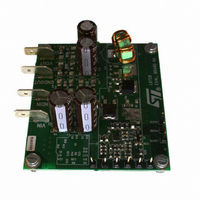
L6728 demonstration board L6728 demonstration board realizes in a four-layer PCB a step-down DC/DC converter and shows the operation of the device in a general purpose application. The input voltage can range from ...
Page 22
A demonstration board Figure 13 demonstration board schematic 22/31 L6728 ...
Page 23
L6728 Table demonstration board - bill of material Qty Capacitors 2 C1 C10 3 C11 to C13 2 C14, C38 2 C15, C19 2 C18, C20 1 C23 1 C24 1 C35 Resistors 4 R1, ...
Page 24
A demonstration board 12.1 Board description 12.1.1 Power input (Vin) This is the input voltage for the power conversion. The High-Side drain is connected to this input. This voltage can range from 1 bus. If ...
Page 25
L6728 demonstration board L6728 demonstration board realizes in a two-layer PCB a step-down DC/DC converter and shows the operation of the device in a general-purpose low-current application. The input voltage can range from ...
Page 26
A demonstration board Figure 17 demonstration board schematic 26/31 OUT OUT OUT OUT OUT OUT OUT OUT OUT OUT OUT OUT OUT OUT OUT OUT COMP GND L6728 ...
Page 27
L6728 Table demonstration board - bill of material Qty Capacitors 2 C12, C51 1 C10 2 C14, C38 1 C39 1 C30 2 C23, C36 1 C24 1 C35 Resistors 3 R1, R2, R17 3 R3, R5, ...
Page 28
A demonstration board If the voltage is between 4.5 V and can supply also the device (through the Vcc pin) and in this case the R16 (0Ω) resistor must be present. 13.1.2 Output (Vout) The output ...
Page 29
L6728 14 Package mechanical data In order to meet environmental requirements, ST offers these devices in ECOPACK® packages. These packages have a lead-free second level interconnect. The category of second level interconnect is marked on the package and on the ...
Page 30
Revision history 15 Revision history Table 9. Document revision history Date 29-Jun-2007 17-Sep-2007 05-Jun-2008 18-Nov-2008 30/31 Revision 1 Initial release 2 Updated T value in Table 3: Thermal data on page 6 J Added Figure 11 on page 21 3 ...
Page 31
... L6728 Information in this document is provided solely in connection with ST products. STMicroelectronics NV and its subsidiaries (“ST”) reserve the right to make changes, corrections, modifications or improvements, to this document, and the products and services described herein at any time, without notice. All ST products are sold pursuant to ST’s terms and conditions of sale. ...