STEVAL-ISA007V1 STMicroelectronics, STEVAL-ISA007V1 Datasheet - Page 9
STEVAL-ISA007V1
Manufacturer Part Number
STEVAL-ISA007V1
Description
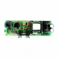
EVAL BOARD 3PH PWR SUPPLY W/ESBT
Manufacturer
STMicroelectronics
Type
DC/DC Switching Converters, Regulators & Controllersr
Datasheets
1.STC08DE150HP.pdf
(9 pages)
2.L5991AD13TR.pdf
(23 pages)
3.STEVAL-ISA007V1.pdf
(5 pages)
Specifications of STEVAL-ISA007V1
Mfg Application Notes
L5991 AppNote
Design Resources
STEVAL-ISA007V1 Gerber Files STEVAL-ISA007V1 Schematic STEVAL-ISA007V1 Bill of Materials
Main Purpose
AC/DC, Primary Side
Outputs And Type
2, Isolated
Power - Output
150W
Voltage - Output
24V, 5V
Current - Output
6.25A, 75mA
Voltage - Input
250 ~ 850V
Regulator Topology
Flyback
Frequency - Switching
90kHz
Board Type
Fully Populated
Utilized Ic / Part
L5991, STC08DE150
Input Voltage
400 V
Output Voltage
5 V, 24 V
Product
Power Management Modules
Lead Free Status / RoHS Status
Contains lead / RoHS non-compliant
For Use With/related Products
L5991, STC08DE150HV
Other names
497-5083


Figure 23. Oscillator and synchronization internal schematic.
The oscillation frequency can be established with
the aid of the diagrams of fig. 14, where R
intended as the parallel of R
operation and R
the following approximate relationships:
which gives the normal operating frequency, and:
which gives the standby frequency, that is the one
the converter will operate at when lightly loaded.
In the above expressions, RA // RB means:
while K
and is related to the duration of the falling-edge of
the sawtooth:
T
ered at pin 1 and defines the upper extreme of the
duty cycle range, D
and calculation) since the output is held low dur-
ing the falling edge.
In case V15 is connected to VREF, however, the
switching frequency will be a half the values taken
d
is also the duration of the sync pulses deliv-
f
R
C
osc
A
T
T
K
f
is defined as:
SB
T
R
T
C
B
d
ST-BY
T
V
RCT
C
90 V
160
REF
30
T
R
T
0.693
A
= R
//
V
4
2
16
0.693 R
x
R
10
15
15
A
B
(see pin 15 for D
STANDBY
9
in standby, or considering
1
1
VREF
GND
R
R
R
A
A
K
A
// R
50
T
A
D1
/OPEN
CLAMP
A
R
R
C
B
B
and R
K
B
T
,
T
K
R3
4 .
T
B
2
X
3 ,
in normal
,
definition
R1
R2
1 ,
T
will be
+
-
from fig. 14 or resulting from (1) and (2).
To prevent the oscillator frequency from switching
back and forth from f
must not exceed 5.5.
If during normal operation the IC is to be synchro-
nized to an external oscillator, R
should be selected for a f
frequency in any condition (typically, 10-20% ),
depending also on the tolerance of the parts.
Pin 3. DC (Duty Cycle Control). By biasing this
pin with a voltage between 1 and 3 V it is possible
to set the maximum duty cycle between 0 and the
upper extreme D
If D
voltage V3 to be applied to pin 3 is:
D
tween V3 and the oscillator ramp (see fig. 24),
thus in case the device is synchronized to an ex-
ternal frequency f
amplitude is reduced), (5) changes into:
A voltage below 1V will inhibit the driver output
stage. This could be used for a not-latched device
disable, for example in case of overvoltage pro-
tection (see application ideas).
If no limitation on the maximum duty cycle is re-
quired (i.e. D
ing. An internal pull-up (see fig. 24) holds the volt-
age above 3V. Should the pin pick up noise (e.g.
max
max
is determined by internal comparison be-
V
3
is the desired maximum duty cycle, the
5 4
MAX
V
3
x
= D
= 5 - 2
ext
(see pin 15).
exp
X
osc
(and therefore the oscillator
), the pin has to be left float-
SYNC
D97IN729A
600 A
(2-Dmax)
to f
osc
R
1
T
SB
lower than the master
D
, the ratio f
C
max
L5991 - L5991A
T
(5)
A
f
ext
, R
D
R
CLK
Q
B
(6)
osc
and C
/ f
9/23
SB
T
Related parts for STEVAL-ISA007V1
Image
Part Number
Description
Manufacturer
Datasheet
Request
R

Part Number:
Description:
BOARD RGB CTR ST7,STP08C596MTR
Manufacturer:
STMicroelectronics
Datasheet:

Part Number:
Description:
Power Management IC Development Tools Full Speed USB to RS232 Bridge Demo
Manufacturer:
STMicroelectronics
Datasheet:
Part Number:
Description:
Power Management IC Development Tools 2.5W solar eval BRD USB SPV1040 LD39050
Manufacturer:
STMicroelectronics
Datasheet:

Part Number:
Description:
BOARD EVAL FOR MEMS SENSORS
Manufacturer:
STMicroelectronics
Datasheet:

Part Number:
Description:
KIT DEV STARTER ST10F276Z5
Manufacturer:
STMicroelectronics
Datasheet:

Part Number:
Description:
BOARD EVAL HDMI $ VIDEO SWITCH
Manufacturer:
STMicroelectronics
Datasheet:

Part Number:
Description:
BOARD DEMO ACCELEROMETER DIL24
Manufacturer:
STMicroelectronics
Datasheet:

Part Number:
Description:
BOARD STLM75/STDS75/ST72F651
Manufacturer:
STMicroelectronics
Datasheet:

Part Number:
Description:
EVAL BOARD 3AXIS MEMS ACCELLRMTR
Manufacturer:
STMicroelectronics
Datasheet:

Part Number:
Description:
BOARD EVAL 8BIT MICRO + TDE1708
Manufacturer:
STMicroelectronics
Datasheet:
Part Number:
Description:
STMicroelectronics [RIPPLE-CARRY BINARY COUNTER/DIVIDERS]
Manufacturer:
STMicroelectronics
Datasheet:
Part Number:
Description:
STMicroelectronics [LIQUID-CRYSTAL DISPLAY DRIVERS]
Manufacturer:
STMicroelectronics
Datasheet:
Part Number:
Description:
BOARD EVAL FOR MEMS SENSORS
Manufacturer:
STMicroelectronics
Datasheet: