NCP30653ABCKGEVB ON Semiconductor, NCP30653ABCKGEVB Datasheet - Page 9
NCP30653ABCKGEVB
Manufacturer Part Number
NCP30653ABCKGEVB
Description
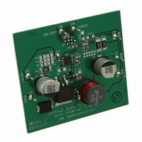
EVAL BOARD FOR NCP30653ABCKG
Manufacturer
ON Semiconductor
Datasheets
1.NCP3065DR2G.pdf
(18 pages)
2.NCP30653ABCKGEVB.pdf
(1 pages)
3.NCP30653ABCKGEVB.pdf
(18 pages)
Specifications of NCP30653ABCKGEVB
Design Resources
NCP3065 Buck Eval Board BOM NCP30653ABCKGEVB Gerber Files NCP3065 Buck Eval Board Schematic
Main Purpose
DC/DC, Step Down
Outputs And Type
1, Non-Isolated
Voltage - Output
3.6V
Current - Output
3A
Voltage - Input
12V
Regulator Topology
Buck
Board Type
Fully Populated
Utilized Ic / Part
NCP30653
Lead Free Status / RoHS Status
Lead free / RoHS Compliant
Power - Output
-
Frequency - Switching
-
Lead Free Status / Rohs Status
Lead free / RoHS Compliant
For Use With/related Products
NCP30653ABCKG
Other names
NCP30653ABCKGEVBOS


of the NCP3065. Two main converter topologies are
demonstrated with actual test data shown below each of the
circuit diagrams.
8. V
9. V
10. The calculated t
The Following Converter Characteristics Must Be Chosen:
less than 10% of the average inductor current I
set by R
converter output current capability.
value since it will directly affect line and load regulation. Capacitor C
electrolytic designed for switching regulator applications.
(See Notes 8, 9, 10)
Figures 16 through 24 show the simplicity and flexibility
V
V
I
DI
f − Maximum output switch frequency.
V
out
out
in
ripple(pp)
SWCE
F
L
I
V
− Output rectifier forward voltage drop. Typical value for 1N5819 Schottky barrier rectifier is 0.4 V.
− Nominal operating input voltage.
pk (Switch)
− Desired output current.
− Desired peak−to−peak inductor ripple current. For maximum output current it is suggested that DI
− Desired output voltage.
ripple(pp)
t on
t off
I
I
L(avg)
out
R
V
SC
t
C
on
− Darlington Switch Collector to Emitter Voltage Drop, refer to Figures 7, 8, 9 and 10.
L
out
SC
T
. If the design goal is to use a minimum inductance value, let DI
− Desired peak−to−peak output ripple voltage. For best performance the ripple voltage should be kept to a low
on
/t
off
must not exceed the minimum guaranteed oscillator charge to discharge ratio.
DI L
V in * V SWCE * V out
V in * V SWCE * V out
V TH
I L(avg) )
I pk (Switch)
Step−Down
V
V out ) V F
f
8 f C O
ref
DI L
t on
t off
0.20
I out
1
L(avg)
R 2
R 1
t on
t off
R
) 1
Figure 16. Design Equations
sense
) 1
DI L
2
. This will help prevent I
2
) (ESR)
http://onsemi.com
APPLICATIONS
C T + 381.6 @ 10
t on
2
9
parameters. Additionally, a complete application design aid
for the NCP3065 can be found at www.onsemi.com.
f osc
Figure 16 gives the relevant design equations for the key
O
*6
should be a low equivalent series resistance (ESR)
pk (Switch)
* 343 @ 10
L
= 2(I
from reaching the current limit threshold
L(avg)
[
*12
V in * V SWCE
t on I out
V out ) V F * V in
). This will proportionally reduce
V in * V SWCE
I out
C O
V TH
I L(avg) )
I pk (Switch)
V
f
Step−Up
ref
DI L
t on
t off
0.20
t on
t off
R 2
R 1
) DI L @ ESR
t on
t off
R
) 1
sense
) 1
) 1
DI L
2
t on
L
be chosen to be
Related parts for NCP30653ABCKGEVB
Image
Part Number
Description
Manufacturer
Datasheet
Request
R

Part Number:
Description:
Up to 1.5 A Constant Current Switching Regulator for LEDs
Manufacturer:
ON Semiconductor
Datasheet:

Part Number:
Description:
EVAL BOARD FOR NCP3065SOBCKG
Manufacturer:
ON Semiconductor
Datasheet:

Part Number:
Description:
EVAL BOARD FOR NCP3065SOBSTG
Manufacturer:
ON Semiconductor
Datasheet:
Part Number:
Description:
ON Semiconductor [VOLTAGE REGULATOR]
Manufacturer:
ON Semiconductor
Datasheet:
Part Number:
Description:
357-036-542-201 CARDEDGE 36POS DL .156 BLK LOPRO
Manufacturer:
ON Semiconductor
Datasheet:
Part Number:
Description:
357-036-542-201 CARDEDGE 36POS DL .156 BLK LOPRO
Manufacturer:
ON Semiconductor
Datasheet:
Part Number:
Description:
357-036-542-201 CARDEDGE 36POS DL .156 BLK LOPRO
Manufacturer:
ON Semiconductor
Datasheet:
Part Number:
Description:
357-036-542-201 CARDEDGE 36POS DL .156 BLK LOPRO
Manufacturer:
ON Semiconductor
Datasheet:
Part Number:
Description:
357-036-542-201 CARDEDGE 36POS DL .156 BLK LOPRO
Manufacturer:
ON Semiconductor
Datasheet:
Part Number:
Description:
357-036-542-201 CARDEDGE 36POS DL .156 BLK LOPRO
Manufacturer:
ON Semiconductor
Datasheet:
Part Number:
Description:
357-036-542-201 CARDEDGE 36POS DL .156 BLK LOPRO
Manufacturer:
ON Semiconductor
Datasheet:
Part Number:
Description:
357-036-542-201 CARDEDGE 36POS DL .156 BLK LOPRO
Manufacturer:
ON Semiconductor
Datasheet:
Part Number:
Description:
357-036-542-201 CARDEDGE 36POS DL .156 BLK LOPRO
Manufacturer:
ON Semiconductor
Datasheet:
Part Number:
Description:
357-036-542-201 CARDEDGE 36POS DL .156 BLK LOPRO
Manufacturer:
ON Semiconductor
Datasheet: