NCP3101BUCK1GEVB ON Semiconductor, NCP3101BUCK1GEVB Datasheet - Page 11
NCP3101BUCK1GEVB
Manufacturer Part Number
NCP3101BUCK1GEVB
Description
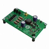
EVAL BOARD FOR NCP3101BUCK1G
Manufacturer
ON Semiconductor
Specifications of NCP3101BUCK1GEVB
Design Resources
NCP3101BUCK1 EVB BOM NCP3101BUCKL1GEVB Gerber Files NCP3101BUCK1 EVB Schematic
Main Purpose
DC/DC, Step Down
Outputs And Type
1, Non-Isolated
Voltage - Output
3.3V
Current - Output
6A
Voltage - Input
13.2V
Regulator Topology
Buck
Frequency - Switching
275kHz
Board Type
Fully Populated
Utilized Ic / Part
NCP3101
Lead Free Status / RoHS Status
Lead free / RoHS Compliant
Power - Output
-
Lead Free Status / Rohs Status
Lead free / RoHS Compliant
For Use With/related Products
NCP3101BUCK1G
Other names
NCP3101BUCK1GEVBOS


Overcurrent Threshold Setting
50 mV to 450 mV by adding a resistor (RSET) between BG
and GND. During a short period of time following V
rising above the UVLO threshold, an internal 10 mA current
(IOCSET) is sourced from the BG pin, creating a voltage
drop across RSET. The voltage drop is compared against a
stepped internal voltage ramp. Once the internal stepped
voltage reaches the RSET voltage, the value is stored
internally until power is cycled. The overall time length for
the OC setting procedure is approximately 3 ms. When
connecting an RSET resistor between BG and GND, the
programmed threshold will be:
I
I
R
R
not connected or the RSET value is too high, the device
switches the OCP threshold to a fixed 96 mV value (5.3 A)
typical at 12 V. The internal safety clamp on BG is triggered
OCSET
OCTH
Switch Node Comparator
DS(on)
SET
The NCP3101C overcurrent threshold can be set from
The RSET values range from 5 kW to 45 kW. If RSET is
I
OCth
SCP Trip Voltage
Figure 24. Switching and Current Limit Timing
LS Gate Drive
HS Gate Drive
+
Switch Node
BG Comparator
SCP Comparator/
C Phase
I
OCSET
Latch Output
2V
2V
2V
R
= Sourced current
= Current trip threshold
= On resistance of the low side MOSFET
= Current set resistor
DS(on)
* R
SET
³ 7.2 A +
10 mA * 13 kW
18 mW
(eq. 1)
http://onsemi.com
CC
11
as soon as BG voltage reaches 700 mV, enabling the 96 mV
fixed threshold and ending the OC setting period. The
current trip threshold tolerance is $25 mV. The accuracy is
best at the highest set point (550 mV). The accuracy will
decrease as the set point decreases.
Drivers
switching MOSFETS with 1 A gate drivers. The gate drivers
also
non−overlap circuitry increases efficiency which minimizes
power dissipation by minimizing the low−side MOSFET
body diode conduction time.
circuitry used is shown in Figure 24.
required to realize the full benefit of the onboard drivers.
The capacitors between V
and CPHS must be placed as close as possible to the IC. A
ground plane should be placed on the closest layer for return
currents to GND in order to reduce loop area and inductance
in the gate drive circuit.
PWM
OUT
The NCP3101C drives the internal high and low side
A block diagram of the non−overlap and gate drive
Careful selection and layout of external components is
include
FAULT
UVLO
Figure 25. Block Diagram
adaptive
UVLO
FAULT
CC
-
-
+
+
non−overlap
and GND and between BST
2 V
2 V
circuitry.
PHASE
BST
TG
V
BG
GND
CC
The
Related parts for NCP3101BUCK1GEVB
Image
Part Number
Description
Manufacturer
Datasheet
Request
R

Part Number:
Description:
Wide Input Voltage Synchronous Buck Converter
Manufacturer:
ON Semiconductor
Datasheet:
Part Number:
Description:
ON Semiconductor [VOLTAGE REGULATOR]
Manufacturer:
ON Semiconductor
Datasheet:
Part Number:
Description:
357-036-542-201 CARDEDGE 36POS DL .156 BLK LOPRO
Manufacturer:
ON Semiconductor
Datasheet:
Part Number:
Description:
357-036-542-201 CARDEDGE 36POS DL .156 BLK LOPRO
Manufacturer:
ON Semiconductor
Datasheet:
Part Number:
Description:
357-036-542-201 CARDEDGE 36POS DL .156 BLK LOPRO
Manufacturer:
ON Semiconductor
Datasheet:
Part Number:
Description:
357-036-542-201 CARDEDGE 36POS DL .156 BLK LOPRO
Manufacturer:
ON Semiconductor
Datasheet:
Part Number:
Description:
357-036-542-201 CARDEDGE 36POS DL .156 BLK LOPRO
Manufacturer:
ON Semiconductor
Datasheet:
Part Number:
Description:
357-036-542-201 CARDEDGE 36POS DL .156 BLK LOPRO
Manufacturer:
ON Semiconductor
Datasheet:
Part Number:
Description:
357-036-542-201 CARDEDGE 36POS DL .156 BLK LOPRO
Manufacturer:
ON Semiconductor
Datasheet:
Part Number:
Description:
357-036-542-201 CARDEDGE 36POS DL .156 BLK LOPRO
Manufacturer:
ON Semiconductor
Datasheet:
Part Number:
Description:
357-036-542-201 CARDEDGE 36POS DL .156 BLK LOPRO
Manufacturer:
ON Semiconductor
Datasheet:
Part Number:
Description:
357-036-542-201 CARDEDGE 36POS DL .156 BLK LOPRO
Manufacturer:
ON Semiconductor
Datasheet:
Part Number:
Description:
Manufacturer:
ON Semiconductor
Datasheet:
Part Number:
Description:
Manufacturer:
ON Semiconductor
Datasheet: