NCP3101BUCK1GEVB ON Semiconductor, NCP3101BUCK1GEVB Datasheet - Page 20
NCP3101BUCK1GEVB
Manufacturer Part Number
NCP3101BUCK1GEVB
Description
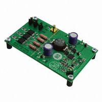
EVAL BOARD FOR NCP3101BUCK1G
Manufacturer
ON Semiconductor
Specifications of NCP3101BUCK1GEVB
Design Resources
NCP3101BUCK1 EVB BOM NCP3101BUCKL1GEVB Gerber Files NCP3101BUCK1 EVB Schematic
Main Purpose
DC/DC, Step Down
Outputs And Type
1, Non-Isolated
Voltage - Output
3.3V
Current - Output
6A
Voltage - Input
13.2V
Regulator Topology
Buck
Frequency - Switching
275kHz
Board Type
Fully Populated
Utilized Ic / Part
NCP3101
Lead Free Status / RoHS Status
Lead free / RoHS Compliant
Power - Output
-
Lead Free Status / Rohs Status
Lead free / RoHS Compliant
For Use With/related Products
NCP3101BUCK1G
Other names
NCP3101BUCK1GEVBOS


used to calculate the transconductance output compensation
network as follows:
C
F
gm
R
R
C
CO
C
f
F
R
CO
C
C
R
Calculating Soft−Start Time
To calculate the soft start delay and soft start time, the
following equations can be used.
C
C
I
The time the output voltage takes to increase from 0 V to a
regulated output voltage is t
cross
SS
PO
LC
C
43.3 nF +
C
1
2
R
5.05 kW +
C
OUT
C
OUT
P
C
P
C
The cross over combined compensation network can be
C
C
ESR
ESR
+
+
2 * 2.35 kHz * 43.3 nF *
F
2 * F
C
309 pF + 820 mF *
t
3.59 ms +
1
PO
SSdelay
P
*
18.9 kHz
LC
+ C
R
= Compensation capacitor
= Pole frequency
= Transconductance of amplifier
= Top of resistor divider
= Bottom of resistor divider
= Crossover frequency
= Compensation resistor
= Compensation resistor
= Soft start current
= Compensation capacitance
= Output capacitor ESR
= Output capacitance
= Output inductor and capacitor frequency
= Output capacitor ESR
= Output capacitor
= Compensation pole capacitor
= Compensation pole capacitor
= Compensation capacitor
* C
2
R
1
* R
OUT
+
2
C
1
*
C
0.309 nF ) 43 nF * 0.83 V
* gm ³
*
*
P
10 kW ) 31.6 kW
2
R
2
CO
) C
) f
C
* 2 * p
ESR
I
cross
1
5.05 kW * 2 * p
SS
10 kW
ss
C
2
2
as shown in Equation 50:
10 mA
* 0.9 V
) 27 kHz * 12 mW * 820 mF
1
12 mW
³
* CO
ESR
* 3.4 mS
* C
OUT
³
(eq. 46)
(eq. 47)
(eq. 48)
(eq. 49)
http://onsemi.com
20
C
C
D
I
t
V
to the bottom of the ramp is considered t
delay time is the addition of the current set delay and t
which in this case is 3.2 ms and 3.59 ms respectively, for a
total of 6.79 ms.
Calculating Input Inrush Current
charging and output charging. The input charging of a buck
stage is usually not controlled, and is limited only by the
input RC network and the output impedance of the upstream
power stage. If the upstream power stage is a perfect voltage
source, then the input charge inrush current can be depicted
as shown in Figure 32 and calculated as:
SS
SS
P
C
ramp
The delay from the charging of the compensation network
The input inrush current has two distinct stages: input
1.31 ms +
Figure 32. Input Charge Inrush Current
Vcomp
t
SS
Vout
IPK
+
= Soft−start current
= Compensation pole capacitor
= Compensation capacitor
= Duty ratio
= Soft−start interval
= Peak−to−peak voltage of the ramp
Figure 31. Soft Start Ramp
0.309 nF ) 43 nF * 27.5% * 1.1 V
C
P
) C
C
I
SS
* D * V
TIME
V
10 mA
ramp
900 mV
³
ss
delay
. The total
(eq. 50)
ss
delay
,
Related parts for NCP3101BUCK1GEVB
Image
Part Number
Description
Manufacturer
Datasheet
Request
R

Part Number:
Description:
Wide Input Voltage Synchronous Buck Converter
Manufacturer:
ON Semiconductor
Datasheet:
Part Number:
Description:
ON Semiconductor [VOLTAGE REGULATOR]
Manufacturer:
ON Semiconductor
Datasheet:
Part Number:
Description:
357-036-542-201 CARDEDGE 36POS DL .156 BLK LOPRO
Manufacturer:
ON Semiconductor
Datasheet:
Part Number:
Description:
357-036-542-201 CARDEDGE 36POS DL .156 BLK LOPRO
Manufacturer:
ON Semiconductor
Datasheet:
Part Number:
Description:
357-036-542-201 CARDEDGE 36POS DL .156 BLK LOPRO
Manufacturer:
ON Semiconductor
Datasheet:
Part Number:
Description:
357-036-542-201 CARDEDGE 36POS DL .156 BLK LOPRO
Manufacturer:
ON Semiconductor
Datasheet:
Part Number:
Description:
357-036-542-201 CARDEDGE 36POS DL .156 BLK LOPRO
Manufacturer:
ON Semiconductor
Datasheet:
Part Number:
Description:
357-036-542-201 CARDEDGE 36POS DL .156 BLK LOPRO
Manufacturer:
ON Semiconductor
Datasheet:
Part Number:
Description:
357-036-542-201 CARDEDGE 36POS DL .156 BLK LOPRO
Manufacturer:
ON Semiconductor
Datasheet:
Part Number:
Description:
357-036-542-201 CARDEDGE 36POS DL .156 BLK LOPRO
Manufacturer:
ON Semiconductor
Datasheet:
Part Number:
Description:
357-036-542-201 CARDEDGE 36POS DL .156 BLK LOPRO
Manufacturer:
ON Semiconductor
Datasheet:
Part Number:
Description:
357-036-542-201 CARDEDGE 36POS DL .156 BLK LOPRO
Manufacturer:
ON Semiconductor
Datasheet:
Part Number:
Description:
Manufacturer:
ON Semiconductor
Datasheet:
Part Number:
Description:
Manufacturer:
ON Semiconductor
Datasheet: