NCP1203GEVB ON Semiconductor, NCP1203GEVB Datasheet - Page 4
NCP1203GEVB
Manufacturer Part Number
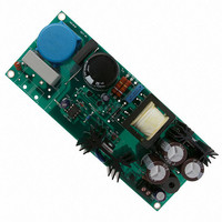
NCP1203GEVB
Description
EVAL BOARD FOR NCP1203G
Manufacturer
ON Semiconductor
Specifications of NCP1203GEVB
Design Resources
NCP1203GEVB BOM NCP1203GEVB Gerber Files NCP1203 EVB Schematic
Main Purpose
AC/DC, Primary Side
Outputs And Type
1, Isolated
Voltage - Output
19V
Current - Output
4A
Voltage - Input
85 ~ 230VAC
Regulator Topology
Flyback
Frequency - Switching
60kHz
Board Type
Fully Populated
Utilized Ic / Part
NPC1200
Lead Free Status / RoHS Status
Lead free / RoHS Compliant
Power - Output
-
Lead Free Status / Rohs Status
Lead free / RoHS Compliant
For Use With/related Products
NCP1203G
Other names
NCP1203GEVBOS


Transformer Calculation
a) you evaluate ALL the transformer parameters, electrical
but also physical ones, including wire type, bobbin stack-up
etc. b) you only evaluate the electrical data and leave the rest
of the process to a transformer manufacturer. We will adhere
to the latest option by providing you with a list of potential
transformer manufacturers you can use for prototyping and
manufacturing. However, as you will discover, designing a
transformer for SMPS is an iterative process: once you
freeze some numbers, it is likely that they finally appear
either over or under estimated. As a result, you re-start with
new values and see if they finally fit your needs. To help you
speed-up the transformer design, a design-aid spreadsheet
is available from the ON Semiconductor web site,
www.onsemi.com/pub/NCP1200. Let’s start the process
with the turn ratio calculation.
Turn Ratio and Output Diode Selection
parameters:
according to the MOSFET BVdss and the diode maximum
reverse voltage. A Schottky diode represents a good choice,
especially with a power supply that can possibly enter
Continuous Conduction Mode (CCM). The lack of reverse
recovery loss and a low forward drop play in favor of this
component. However, because of the metal-silicon
junction, moderate breakdown voltages are available for a
moderate cost. The MBR20100 represents an interesting
choice since it welcomes two 100 V Schottky in a TO-220
package. Being in thermal contact, a parallel wiring is
possible. The 100 V V
turn ratio we can go down to, keeping an acceptable safety
margin:
adequate safety margin (Vreverse = 80 V max). The diode’s
Transformer calculation can be done in several manners:
The primary/secondary turn ratio affects several
With these numbers in mind, you can tweak the turn ratio
The drain plateau voltage during the OFF time: the
lowest plateau gives room for the leakage inductance
spike before reaching the MOSFET’s BVdss:
The secondary Peak Inverse Voltage (PIV) is linked to
the turn ratio and the regulated output voltage by:
If you lower the plateau voltage, you will increase the
reverse voltage the secondary diode must sustain.
Np:Ns
Vplateau +
PIV + Ns
1:0.221. A final ratio of 1:0.166 offers an
Np
Ns
Np
N + PIV * Vout
RRM
@ (Vout ) Vf) ) VinDC max
@ VinDC max ) Vout
VinDC max
lets us calculate the minimum
http://onsemi.com
AND8076/D
(10)
(12)
(11)
4
conduction power is evaluating using the following
formula:
Rather than manually calculating these numbers, we will see
later on how a Spice simulator can do the job for us.
Primary Inductance and Peak Current
a small place, it is of common practice to make the power
supply enter CCM in the middle of the total AC range
(around 180 VAC in our case). When the input AC voltage
diminishes, the on-time increases and the primary /
secondary RMS current go up. This implies a greater
heatsink for the MOSFET but also larger aluminum cans for
the secondary filters. For this reason, a transition from
Discontinuous Conduction Mode (DCM) to CCM will be
envisaged here. Figure 5 depicts these different modes.
Different methods exist to find the point transition takes
place (also called the critical or borderline point). The idea
consists in finding the critical inductance Lc that will make
the supply enter CCM at 180 VAC. From Figure 5, we can
write:
Figure 5. Depending on the Primary Current at Turn- On,
For AC/DC adapters delivering this amount of power in
I
L(avg)
the Supply Crosses Various Operating Modes
I
L
Pdiode avg + Vf @ Id avg ) Rd @ Id rms 2
ON
I
D/Fs
P
ton +
toff +
Not 0 at
turn ON
BCM
OFF
time
L = Lc
Lp @ Ip
VinDC
N @ (Vout ) Vf)
Dead-time
Lp @ Ip
CCM
0 before
turn ON
L > Lc
L > Lc
DCM
0
0
(13)
(14)
(15)
Related parts for NCP1203GEVB
Image
Part Number
Description
Manufacturer
Datasheet
Request
R

Part Number:
Description:
Current Mode Controller Fixed Frequency Operation
Manufacturer:
ON Semiconductor
Datasheet:
Part Number:
Description:
ON Semiconductor [VOLTAGE REGULATOR]
Manufacturer:
ON Semiconductor
Datasheet:
Part Number:
Description:
357-036-542-201 CARDEDGE 36POS DL .156 BLK LOPRO
Manufacturer:
ON Semiconductor
Datasheet:
Part Number:
Description:
357-036-542-201 CARDEDGE 36POS DL .156 BLK LOPRO
Manufacturer:
ON Semiconductor
Datasheet:
Part Number:
Description:
357-036-542-201 CARDEDGE 36POS DL .156 BLK LOPRO
Manufacturer:
ON Semiconductor
Datasheet:
Part Number:
Description:
357-036-542-201 CARDEDGE 36POS DL .156 BLK LOPRO
Manufacturer:
ON Semiconductor
Datasheet:
Part Number:
Description:
357-036-542-201 CARDEDGE 36POS DL .156 BLK LOPRO
Manufacturer:
ON Semiconductor
Datasheet:
Part Number:
Description:
357-036-542-201 CARDEDGE 36POS DL .156 BLK LOPRO
Manufacturer:
ON Semiconductor
Datasheet:
Part Number:
Description:
357-036-542-201 CARDEDGE 36POS DL .156 BLK LOPRO
Manufacturer:
ON Semiconductor
Datasheet:
Part Number:
Description:
357-036-542-201 CARDEDGE 36POS DL .156 BLK LOPRO
Manufacturer:
ON Semiconductor
Datasheet:
Part Number:
Description:
357-036-542-201 CARDEDGE 36POS DL .156 BLK LOPRO
Manufacturer:
ON Semiconductor
Datasheet:
Part Number:
Description:
357-036-542-201 CARDEDGE 36POS DL .156 BLK LOPRO
Manufacturer:
ON Semiconductor
Datasheet:
Part Number:
Description:
Manufacturer:
ON Semiconductor
Datasheet:
Part Number:
Description:
Manufacturer:
ON Semiconductor
Datasheet: