NCP1351ADAPGEVB ON Semiconductor, NCP1351ADAPGEVB Datasheet
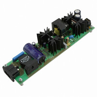
EVAL BOARD FOR NCP1351ADAPG

NCP1351ADAPGEVB

Manufacturer Part Number
NCP1351ADAPGEVB
Description
EVAL BOARD FOR NCP1351ADAPG
Manufacturer
ON Semiconductor

Specifications of NCP1351ADAPGEVB

Design Resources
NCP1351 Adapter EVB BOM NCP1351ADAPGEVB Gerber Files NCP1351 Adapter EVB Schematic
Main Purpose
AC/DC, Primary Side
Outputs And Type
1, Isolated
Power - Output
57W
Voltage - Output
19V
Current - Output
3A
Voltage - Input
90 ~ 265VAC
Regulator Topology
Flyback
Frequency - Switching
65kHz
Board Type
Fully Populated
Utilized Ic / Part
NCP1351
Lead Free Status / RoHS Status
Lead free / RoHS Compliant
Other names
NCP1351ADAPGEVBOS
AND8263/D
NCP1351 Evaluation Board,
a 19 V − 3 A Adapter
Prepared by: Nicolas Cyr, Christophe Basso
ON Semiconductor
The NCP1351 at a Glance
implementing a fixed peak current mode control (hence the
more appropriate term “quasi−fixed” t
modulates the off time duration according to the output
power demand. In high power conditions, the switching
frequency increases until a maximum is hit. This upper limit
depends on an external capacitor selected by the designer. In
light load conditions, the off time expands and the NCP1351
operates at a lower frequency. As the frequency reduces, the
contribution of all frequency−dependent losses accordingly
goes down (driver current, drain capacitive losses, switching
losses), naturally improving the efficiency at various load
levels.
the frequency will certainly force the converter to operate
into the audible region. To prevent the transformer
mechanical resonance, the NCP1351 gradually reduces –
compresses – the peak current setpoint as the load becomes
lighter. When the current reaches 30% of the nominal value,
the compression stops and the off duration keeps expanding
towards low frequencies.
offers an excellent solution for designers looking for low
standby power converters. Also, compared to the skip−cycle
method, the smooth off time expansion does not bring
additional ripple in no−load conditions: the output voltage
remains quiet.
of operation improves the EMI signature since the switching
frequency varies with the natural bulk ripple voltage.
proprietary circuitry, the NCP1351 startup section does not
consumme more than 10 mA during the startup sequence.
The designer can thus easily combine startup time and
standby consumption.
designer knows the pain of building converters where a
precise over current limit must be obtained. When the fault
detection relies on the auxiliary V
increases. Here, the NCP1351 observes the lack of feedback
current starts a timer to countdown. At the end of its charge,
© Semiconductor Components Industries, LLC, 2006
October, 2006 − Rev. 1
Fixed
Peak Current Compression at Light Loads: Reducing
Low Standby−power: the frequency reduction technique
Natural Frequency Dithering: the quasi−fixed t
Extremely Low Start−up Current: built on a
Overload Protection Based on Fault Timer: every
t
on
,
variable
t
off
current−mode
CC
on
, the pain even
), the NCP1351
on
control:
mode
1
the timer either triggers an auto−recovery sequence
(auto−restart, B version) or permanently latches−off (A).
externally trigger the latch to build additional protections
such as over−voltage (OVP) or over−temperature (OTP).
The Schematic
Input voltage: 90 – 265 Vac
Output voltage: 19 V @ 3 A
Over voltage protection
Over power protection
Auto−recovery short−circuit protection
switching frequency has become an industry standard for the
vast majority of power supplies connected on the mains.
With the NCP1351, selecting a C
the upper limit to 65 kHz. As a result, when the controller
detects a need for a higher frequency, implying an overload
condition, it will start to charge the timer capacitor: if the
overload disappears, the timer capacitor goes back to zero.
If the fault remains, the timer capacitor voltage reaches 5 V
and starts the auto−recovery process.
recommendations described in the NCP1351 data−sheet.
We came−up to the following values:
L
N
N
from the ON Semiconductor website which also gives
transformer parameters. The core is a PQ26x25 made of a
3F3 material and has been manufactured by Delta
Electronics (reference 86H−6232). The leakage inductance
is kept around 1%, leading to a good efficiency and reduced
losses in no−load conditions. The schematic appears on
Figure 2. The converter operates in CCM with a 40%
duty−cycle at low mains and stays CCM at high line. Despite
the frequency variation, it is possible to evaluate the input
voltage point at which the converter leaves CCM:
p
p
p
Latch Fault Input: a dedicated input lets the designer
The design must fullfil the following specifications:
Offering a good EMI signature, the 65 kHz maximum
The transformer has been derived using the design
It is also possible to use the Excel
:N
:N
= 770 mH
s
aux
= 1:0.25
= 1:0.18
APPLICATION NOTE
http://onsemi.com
t
capacitor of 270 pF fixes
Publication Order Number:
®
spreadsheet available
AND8263/D

Related parts for NCP1351ADAPGEVB

NCP1351ADAPGEVB Summary of contents

Page 1

... It is also possible to use the Excel from the ON Semiconductor website which also gives transformer parameters. The core is a PQ26x25 made of a 3F3 material and has been manufactured by Delta Electronics (reference 86H−6232). The leakage inductance is kept around 1%, leading to a good efficiency and reduced losses in no− ...

Page 2

V in, crit + I peak V out h * 2NP out Where the selected peak current in the inductor peak V , the output voltage out η, the converter efficiency P , the delivered power out N, ...

Page 3

The overvoltage protection uses zener diode (D connected to the auxiliary V . When the voltage on this rail CC exceeds 15 V plus the NCP1351 5 V latch trip point (total is thus 20 V), the ...

Page 4

OUT 0.5 Output Power 0.5 W No−load Power No−load Overpower Protection Level OUT Overpower Start−up Time OUT Start−up Duration On the above arrays, we can see ...

Page 5

pin8 pin8 Figure 7. Startup Sequence to Test the Margin on the 100 ms Timer Vac the above picture, a short−circuit has been made at the highest line ...

Page 6

Figure 10. The Drain−source Waveform at Different Output Currents ( and 1 A). The Input Voltage is 230 Vac Figure 11. Short−circuit on the Optocoupler LED The output voltage increases and then the controller ...

Page 7

V V out out Figure 12. Load Step from 0 with Slew−rate from a 90 Vac V V out out Figure 13. Load Step from 0 with ...

Page 8

... Panasonic 5% SMD 0805 PHYCOMP 5% SOT23 ON Semiconductor 0% axial ON Semiconductor 0% axial ON Semiconductor 0% TO220 ON Semiconductor 0% axial Semiconductor 0% SOD−123 ON Semiconductor 6.2 °C/W 0% radial 2% TO92 ON Semiconductor 0% radial Multicomp 230 Vac/ 0% radial 2/” 0% rad5.08mm Weidmuller 0% radial Schaffner 0% radial Wurth Elektronik 0% TO220 0% TO92 ON Semiconductor 1% SOT23 5% axial 2% SMD 1206 ...

Page 9

... NC SMD 1206 2% SMD 1206 2% SMD 1206 2% SMD 1206 2% SMD 1206 2% SMD 1206 2% SMD 1206 FIX 4 H radial sfh6156/ SMD SO−8 ON Semiconductor http://onsemi.com 9 Sub- Manufacturer Part stitution Number Allowed yes Welwyn WCR12063K92% yes Welwyn WCR120610R2% yes Welwyn WCR12061K52% yes Welwyn WCR120647K2% ...

Page 10

... Opportunity/Affirmative Action Employer. This literature is subject to all applicable copyright laws and is not for resale in any manner. PUBLICATION ORDERING INFORMATION LITERATURE FULFILLMENT: Literature Distribution Center for ON Semiconductor P.O. Box 5163, Denver, Colorado 80217 USA Phone: 303−675−2175 or 800−344−3860 Toll Free USA/Canada Fax: 303− ...

Related keywords