NCP1351ADAPGEVB ON Semiconductor, NCP1351ADAPGEVB Datasheet - Page 2
NCP1351ADAPGEVB
Manufacturer Part Number
NCP1351ADAPGEVB
Description
EVAL BOARD FOR NCP1351ADAPG
Manufacturer
ON Semiconductor
Datasheets
1.NCP1351APG.pdf
(27 pages)
2.NCP1351ADAPGEVB.pdf
(10 pages)
3.NCP1351ADAPGEVB.pdf
(1 pages)
Specifications of NCP1351ADAPGEVB
Design Resources
NCP1351 Adapter EVB BOM NCP1351ADAPGEVB Gerber Files NCP1351 Adapter EVB Schematic
Main Purpose
AC/DC, Primary Side
Outputs And Type
1, Isolated
Power - Output
57W
Voltage - Output
19V
Current - Output
3A
Voltage - Input
90 ~ 265VAC
Regulator Topology
Flyback
Frequency - Switching
65kHz
Board Type
Fully Populated
Utilized Ic / Part
NCP1351
Lead Free Status / RoHS Status
Lead free / RoHS Compliant
Other names
NCP1351ADAPGEVBOS


Where:
I
V
η, the converter efficiency
P
N, the transformer turn ratio, N
converter will always be in CCM at full power. To the
opposite, we can also predict the power level at which the
converter leaves CCM at low and high line conditions:
DCM for an output power below 42 W. When the voltage
increases to 330 Vdc, the power level at which CCM is
excited is 55 W.
the 4.7 mF capacitor (C
Despite a small value for C
no−load conditions thanks to the split configuration:
peak
out
out
J1 1
Since we are limited to 265 Vac, we can see that the
For an input voltage of 120 Vdc, the converter enters
Two 1 MW resistors ensure a clean start−up sequence with
, the delivered power
, the output voltage
is the selected peak current in the inductor
2
5.1 kW
R6b
R6a
220 nF
R15
C11
X2
1 W
1 W
100 nF
1 W
1 W
C4
RN114−
P out, crit +
0.8/02
L1
2.5 kW
R5
V in, crit +
3
C15
), directly from the bulk capacitor.
C8
220 pF
opto_e
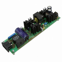
Figure 2. The 57 W Adapter Board Featuring the NCP1351 Controller
−
hI peak V in V out
V out ) NV in
3
, the V
~
p
~
47 pF
C14
:N
1N4148
I peak V out h * 2NP out
22 pF
1
2
3
4
IC4
KBU4K
100 kW
s
+
= 1:N
OPP or no OPP
U2
D9
R19
CC
2P out V out
still maintains in
NCP1351
8
7
6
5
R1
C9
+
100 V
C18
150 kW
270 pF
R20
C12
400 V
100 nF
2.2 kW
100 mF
1 MW
2
1
R7
(eq. 2)
http://onsemi.com
J3
JUMPER
220 nF
100 nF
47 kW 47 kW
15 V
C10
+
1 MW
R2
100 mF
opto_c
R13
2
C1
D1
0
2
+
19
10
R16
1N4148
BC857
4.7 mF
C17
R11
35 V
period of time (CV
second, larger capacitor (C
standby.
300 mA via R
TL431. 1 mA at least must flow in the TL431 in worse case
conditions (full load). Failure to respect this will degrade the
power supply output impedance and regulation will suffer.
A 1.5 kW has proven to do just well, without degrading the
standby power.
C3
D6
The split V
The primary−side feedback current is fixed to roughly
+
2
35 V
Q1
0.9 * 2
1N4148
1N4937
D2
MUR160
57
400 V
C2
D3
D8
10 nF
47 kW
19
R18
CC
0
5
0.25
M1
and an additional bias is provided for the
86H−6232
T1
Vcc
configuration helps to start−up in a small
CC
4 A / 600 V
SPP04N60C3
0.1 mF
57
to charge alone) but the addition of a
MBR20100
1 mF
bulk
SFH6156−2
C5
C5a
opto_e
Figure 1.
25 V
opto_c
+ 380 Vdc
+
D5
R1
R2
CVcc
U1
+
C13
Y1
res
2.2 nF
4
3
+
), ensures enough V
out
1 mF
25 V
C5b
+
Cres
220 mF
1 kW
IC2
2.2 mH
L2
R8
TL431
R17
1.5 kW
C6
25 V
C7
100 nF
R14
NC
+
10 kW
27 kW
39 kW
(eq. 1)
R12
R10
R9
2
1
CC
J2
in
Related parts for NCP1351ADAPGEVB
Image
Part Number
Description
Manufacturer
Datasheet
Request
R

Part Number:
Description:
ON Semiconductor [VOLTAGE REGULATOR]
Manufacturer:
ON Semiconductor
Datasheet:
Part Number:
Description:
357-036-542-201 CARDEDGE 36POS DL .156 BLK LOPRO
Manufacturer:
ON Semiconductor
Datasheet:
Part Number:
Description:
357-036-542-201 CARDEDGE 36POS DL .156 BLK LOPRO
Manufacturer:
ON Semiconductor
Datasheet:
Part Number:
Description:
357-036-542-201 CARDEDGE 36POS DL .156 BLK LOPRO
Manufacturer:
ON Semiconductor
Datasheet:
Part Number:
Description:
357-036-542-201 CARDEDGE 36POS DL .156 BLK LOPRO
Manufacturer:
ON Semiconductor
Datasheet:
Part Number:
Description:
357-036-542-201 CARDEDGE 36POS DL .156 BLK LOPRO
Manufacturer:
ON Semiconductor
Datasheet:
Part Number:
Description:
357-036-542-201 CARDEDGE 36POS DL .156 BLK LOPRO
Manufacturer:
ON Semiconductor
Datasheet:
Part Number:
Description:
357-036-542-201 CARDEDGE 36POS DL .156 BLK LOPRO
Manufacturer:
ON Semiconductor
Datasheet:
Part Number:
Description:
357-036-542-201 CARDEDGE 36POS DL .156 BLK LOPRO
Manufacturer:
ON Semiconductor
Datasheet:
Part Number:
Description:
357-036-542-201 CARDEDGE 36POS DL .156 BLK LOPRO
Manufacturer:
ON Semiconductor
Datasheet:
Part Number:
Description:
357-036-542-201 CARDEDGE 36POS DL .156 BLK LOPRO
Manufacturer:
ON Semiconductor
Datasheet:
Part Number:
Description:
Manufacturer:
ON Semiconductor
Datasheet:
Part Number:
Description:
Manufacturer:
ON Semiconductor
Datasheet: