NCP1230GEVB ON Semiconductor, NCP1230GEVB Datasheet - Page 14
NCP1230GEVB
Manufacturer Part Number
NCP1230GEVB
Description
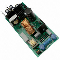
EVAL BOARD FOR NCP1230G
Manufacturer
ON Semiconductor
Specifications of NCP1230GEVB
Design Resources
NCP1230 EVB BOM NCP1230GEVB Gerber Files NCP1230 EVB Schematic
Main Purpose
AC/DC, Primary Side
Outputs And Type
1, Isolated
Power - Output
90W
Voltage - Output
18.6V
Current - Output
4.74A
Voltage - Input
85 ~ 265VAC
Regulator Topology
Flyback
Frequency - Switching
47kHz
Board Type
Fully Populated
Utilized Ic / Part
NCP1230
Lead Free Status / RoHS Status
Lead free / RoHS Compliant
For Use With/related Products
NCP1230G
Other names
NCP1230GEVBOS


Leading Edge Blanking
large current spike at the beginning of the current ramp due
to the Power Switch gate to source capacitance, transformer
interwinding capacitance, and output rectifier recovery
time. To prevent prematurely turning off the PWM drive
output, a Leading Edges Blanking (LEB) (Figure 34) circuit
is place is series with the current sense input, and PWM
comparator. The LEB circuit masks the first 250 ns of the
current sense signal.
Short−Circuit Condition
use an auxiliary windings to detect events on the isolated
secondary output. There maybe some conditions (for
example when the leakage inductance is high) where it can
be extremely difficult to implement short−circuit and
overload protection. This occurs because when the power
switch opens, the leakage inductance superimposes a large
spike on the switch drain voltage. This spike is seen on the
3
In Switch Mode Power Supplies (SMPS) there can be a
The NCP1230 is different from other controllers which
CS
2.3 Vpp
Ramp
18 k
10 V
LEB
3 V
FB/3
250 ns
PWM Comparator
Thermal Shutdown
Figure 34.
125 msec Timer
-
+
+
-
Latch−Off
Vccreset
Skip
R
S
Q
http://onsemi.com
14
isolated secondary output and on the auxiliary winding.
Because the auxiliary winding and diode form a peak
rectifier, the auxiliary Vcc capacitor voltage can be charged
up to the peak value rather than the true plateau which is
proportional to the output level.
error flag. As soon as the internal 1.0 V error flag is asserted
high, a 125 ms timer starts. If at the end of the 125 ms timeout
period, the error flag is still asserted then the controller
determines that there is a true fault condition and stops the
PWM drive output, refer to Figure 35. When this occurs,
Vcc starts to decrease because the power supply is locked
out. When Vcc drops below UVLOlow (7.7 V typical), it
enters a latch−off phase where the internal consumption is
reduced down to 680 mA (typical). The voltage on the Vcc
capacitor continues to drop, but at a lower rate. When Vcc
reaches the latch−off level (5.6 V), the current source is
turned on and pulls Vcc above UVLOhigh. To limit the fault
output power, a divide−by−two circuit is connected to the
Vcc pin that requires two startup sequences before
attempting to restart the power supply. If the fault has gone
and the error flag is low, the controller resumes normal
operations.
asserted, the error flag will normally drop prior to the 125 ms
timeout period and the controller continues to operate
normally.
Skip Mode, SW1 opens and the PFC_Vcc output will shut
down and will not be activated until the fault goes away and
the power supply resumes normal operations.
is desirable for the Burst duty cycle to be kept below
20%(the burst duty−cycle is defined as Tpulse / Tfault).
To resolve these issues the NCP1230 monitors the 1.0 V
Under transient load conditions, if the error flag is
If the 125 msec timer expires while the NCP1230 is in the
While in the Skip Mode, to avoid any thermal runaway it
Related parts for NCP1230GEVB
Image
Part Number
Description
Manufacturer
Datasheet
Request
R

Part Number:
Description:
Fixed Frequency Controller Featuring Pfc Go To Standby Function
Manufacturer:
ON Semiconductor
Datasheet:
Part Number:
Description:
ON Semiconductor [VOLTAGE REGULATOR]
Manufacturer:
ON Semiconductor
Datasheet:
Part Number:
Description:
357-036-542-201 CARDEDGE 36POS DL .156 BLK LOPRO
Manufacturer:
ON Semiconductor
Datasheet:
Part Number:
Description:
357-036-542-201 CARDEDGE 36POS DL .156 BLK LOPRO
Manufacturer:
ON Semiconductor
Datasheet:
Part Number:
Description:
357-036-542-201 CARDEDGE 36POS DL .156 BLK LOPRO
Manufacturer:
ON Semiconductor
Datasheet:
Part Number:
Description:
357-036-542-201 CARDEDGE 36POS DL .156 BLK LOPRO
Manufacturer:
ON Semiconductor
Datasheet:
Part Number:
Description:
357-036-542-201 CARDEDGE 36POS DL .156 BLK LOPRO
Manufacturer:
ON Semiconductor
Datasheet:
Part Number:
Description:
357-036-542-201 CARDEDGE 36POS DL .156 BLK LOPRO
Manufacturer:
ON Semiconductor
Datasheet:
Part Number:
Description:
357-036-542-201 CARDEDGE 36POS DL .156 BLK LOPRO
Manufacturer:
ON Semiconductor
Datasheet:
Part Number:
Description:
357-036-542-201 CARDEDGE 36POS DL .156 BLK LOPRO
Manufacturer:
ON Semiconductor
Datasheet:
Part Number:
Description:
357-036-542-201 CARDEDGE 36POS DL .156 BLK LOPRO
Manufacturer:
ON Semiconductor
Datasheet:
Part Number:
Description:
357-036-542-201 CARDEDGE 36POS DL .156 BLK LOPRO
Manufacturer:
ON Semiconductor
Datasheet:
Part Number:
Description:
Manufacturer:
ON Semiconductor
Datasheet:
Part Number:
Description:
Manufacturer:
ON Semiconductor
Datasheet: