STEVAL-ISA024V1 STMicroelectronics, STEVAL-ISA024V1 Datasheet
STEVAL-ISA024V1
Specifications of STEVAL-ISA024V1


Related parts for STEVAL-ISA024V1


STEVAL-ISA024V1 Summary of contents
Page 1
Features ■ Input voltage range from 1.8V to 18V ■ Supply voltage range from 4.5V to 18V ■ Adjustable output voltage down to 0.6V with ±0.8% accuracy over line voltage and temperature (0°C~125°C) ■ Fixed frequency voltage mode control ■ ...
Page 2
Contents Contents 1 Summary description . . . . . . . . . . . . . . . . . . . . . . . . . . . . . . . . . . . ...
Page 3
L6725 - L6725A 5.11 Synchronization . . . . . . . . . . . . . . . . . . . . . . . . . . . . . . . . . . . ...
Page 4
Summary description 1 Summary description The device is a flexible high performance PWM buck controller dedicated for low voltage distributed DC-DC. The input voltage can range from 1.8V to 18V, while the supply voltage can range from 4.5V to 18V. ...
Page 5
L6725 - L6725A 2 Electrical data 2.1 Maximum rating Table 2. Absolute maximum ratings Symbol GND and PGND, OCH Boot voltage BOOT - PHASE V V HGATE - PHASE V BOOT BOOT PHASE ...
Page 6
Pin connections and functions 3 Pin connections and functions Figure 2. Pins connection (top view) COMP SS/INH EAREF OCL OCH PHASE HGATE BOOT Table 4. Pin functions Pin n° Name This pin is connected to the error amplifier output and ...
Page 7
L6725 - L6725A Table 4. Pin functions Pin n° Name A resistor connected from this pin and the high-side MOSFET(s) drain sets the peak- current-limit. The peak current is sensed through the high-side MOSFET(s). The internal 100µA current generator (I ...
Page 8
Electrical characteristics 4 Electrical characteristics V = 12V 25°C unless otherwise specified Table 5. Electrical characteristics Symbol Parameter V supply current CC V Stand by current quiescent current CC Power-ON Turn-ON V ...
Page 9
L6725 - L6725A Table 5. Electrical characteristics Symbol Parameter Error Amplifier R EAREF Input Resistance EAREF I I.I. bias current FB Ext Ref Clamp V Error amplifier offset OFFSET G Open Loop Voltage Gain V GBWP Gain-Bandwidth Product SR Slew-Rate ...
Page 10
L6725 - L6725A 5 Device description The controller provides complete control logic and protection for flexible and cost-effective DC- DC converters designed to drive N-Channel MOSFETs in a synchronous rectified buck topology. The output voltage of the converter ...
Page 11
L6725 - L6725A 5.3 Bypassing the LDO to avoid the voltage drop with low Vcc ≈ the internal LDO works in dropout with an output resistance of about 1Ω. The CC maximum LDO output current is about ...
Page 12
Device description 5.5 Error amplifier Figure 4. Error amplifier reference 5.6 Soft start When both V and V CC the start-up phase takes place. Otherwise the SS pin is internally shorted to GND. At start-up, a ramp is generated charging ...
Page 13
L6725 - L6725A L6725:The output of the error amplifier is clamped with this voltage (VSS) until it reaches the programmed value. L6725A:The reference of the error amplifier is clamped with this voltage (VSS) until it reaches the programmed value. No ...
Page 14
Device description 5.7 Driver section The high-side and low-side drivers allow using different types of power MOSFETs (also multiple MOSFETs to reduce the R supplied by V while the high-side driver is supplied by the BOOT pin. A predictive dead ...
Page 15
L6725 - L6725A 5.9 Hiccup mode Figure 9. Constant current and Hiccup Mode during an OCP. During the soft-start phase the OCP provides a constant-current-protection. If during the T the OCH comparator triggers an over current the high-side MOSFET(s) is ...
Page 16
Device description 5.11 Synchronization The presence of many converters on the same board can generate beating frequency noise. To avoid this it is important to make them operate at the same switching frequency. Moreover, a phase shift between different modules ...
Page 17
L6725 - L6725A 5.12 Bootstrap anti-discharging system This built-in system avoids that the voltage across the bootstrap capacitor becomes less than 3.3V. An internal comparator senses the voltage across the external bootstrap capacitor keeping it charged, eventually turning-on the low-side ...
Page 18
Application details 6 Application details 6.1 Inductor design The inductance value is defined by a compromise between the transient response time, the efficiency, the cost and the size. The inductor has to be calculated to sustain the output and the ...
Page 19
L6725 - L6725A 6.2 Output capacitors The output capacitors are basic components for the fast transient response of the power supply. For example, during a positive load transient, they supply the current to the load until the converter reacts. The ...
Page 20
Application details 6.4 Compensation network The loop is based on a voltage mode control internal/external reference voltage and scaled by the external resistor divider. The error amplifier output V COMP pulse-width modulated (PWM) with an amplitude of V filtered by ...
Page 21
L6725 - L6725A ● Modulator singularity frequencies: ω LC ● Compensation network singularity frequencies: ω ω ● Compensation network design: – Put the gain R ω – Place Z1 ω – ...
Page 22
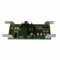
Demoboard 7 Demoboard 7.1 20A board description L6725 demoboard realizes in a four layer PCB a step-down DC/DC converter and shows the operation of the device in a general purpose application. The input voltage can range from 4.5V to 14V ...
Page 23
L6725 - L6725A Table 6. Demoboard part list Reference Value R1 1kΩ R2 1kΩ R3 4K7 N.C. R7 2KΩ R8 10Ω R9 1KΩ R10 2.2Ω R11 2.2Ω R12 N.C. C1 4.7nF C2 47nF C3 1nF C4 100nF ...
Page 24
Demoboard Table 7. Other inductor manufacturer Manufacturer WURTH ELEKTRONIC SUMIDA EPCOS TDK TOKO COILTRONICS Table 8. Other capacitor manufacturer Manufacturer TDK NIPPON CHEMI-CON PANASONIC Figure 17. Demoboard efficiency ...
Page 25
L6725 - L6725A Figure 18. PCB Layout: top layer Figure 19. PCB Layout: power ground layer Figure 20. PCB Layout: signal-ground layer Demoboard 25/32 ...
Page 26
Demoboard 7.2 5A board description L6725 demoboard realizes in a two layer PCB a step-down DC/DC converter and shows the operation of the device in a general purpose application. The input voltage can range from 4.5V to 14V and the ...
Page 27
L6725 - L6725A Table 9. Demoboard part list Reference Value C15 N.C. C16-19 2X 330uF 2,7uH L1 DO3316P-272HC D1 STPS1L30M D3 N.C. STS8DNH3LL Q1 (Dual Mosfet) U1 L6725 Figure 21. Demoboard efficiency ...
Page 28
Demoboard Figure 22. Demoboard layout Figure 23. Demoboard layout 28/32 L6725 - L6725A ...
Page 29
L6725 - L6725A 8 Package mechanical data In order to meet environmental requirements, ST offers these devices in ECOPACK These packages have a Lead-free second level interconnect . The category of second Level Interconnect is marked on the package and ...
Page 30
Package mechanical data Table 10. SO16N mechanical data Dim Min 0. ( (1) 3 4. "D" and "F" ...
Page 31
L6725 - L6725A 9 Revision history Table 11. Revision history Date Revision 20-Dec-2005 30-May-2006 26-Jun-2006 5-Oct-2006 28-Jun-2007 1 Initial release. 2 New template, thermal data updated 3 Note page 5 deleted 4 Added new orderable L6725A, and 5A demoboard 5 ...
Page 32
... Information in this document is provided solely in connection with ST products. STMicroelectronics NV and its subsidiaries (“ST”) reserve the right to make changes, corrections, modifications or improvements, to this document, and the products and services described herein at any time, without notice. All ST products are sold pursuant to ST’s terms and conditions of sale. ...