LM2831XMF EVAL National Semiconductor, LM2831XMF EVAL Datasheet - Page 13
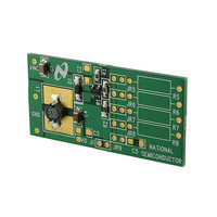
LM2831XMF EVAL
Manufacturer Part Number
LM2831XMF EVAL
Description
EVAL BOARD FOR LM2831XMF
Manufacturer
National Semiconductor
Specifications of LM2831XMF EVAL
Main Purpose
DC/DC, Step Down
Outputs And Type
1, Non-Isolated
Voltage - Output
0.6 ~ 5.5V
Current - Output
1.5A
Voltage - Input
3 ~ 5.5V
Regulator Topology
Buck
Frequency - Switching
1.6MHz
Board Type
Fully Populated
Utilized Ic / Part
LM2831
Lead Free Status / RoHS Status
Contains lead / RoHS non-compliant
Power - Output
-
Other names
*LM2831XMF EVAL
LM2831XMFEVAL
LM2831XMFEVAL


Design Guide
significantly with little detriment to the regulator stability. Like
the input capacitor, recommended multilayer ceramic ca-
pacitors are X7R or X5R types.
CATCH DIODE
The catch diode (D1) conducts during the switch off-time. A
Schottky diode is recommended for its fast switching times
and low forward voltage drop. The catch diode should be
chosen so that its current rating is greater than:
The reverse breakdown rating of the diode must be at least
the maximum input voltage plus appropriate margin. To im-
prove efficiency, choose a Schottky diode with a low forward
voltage drop.
OUTPUT VOLTAGE
The output voltage is set using the following equation where
R2 is connected between the FB pin and GND, and R1 is
connected between V
is 10k. When designing a unity gain converter (Vo = 0.6V),
R1 should be between 0Ω and 100Ω, and R2 should be
equal or greater than 10kΩ.
I
D1
O
V
and the FB pin. A good value for R2
REF
= I
(Continued)
OUT
= 0.60V
x (1-D)
13
PCB LAYOUT CONSIDERATIONS
When planning layout there are a few things to consider
when trying to achieve a clean, regulated output. The most
important consideration is the close coupling of the GND
connections of the input capacitor and the catch diode D1.
These ground ends should be close to one another and be
connected to the GND plane with at least two through-holes.
Place these components as close to the IC as possible. Next
in importance is the location of the GND connection of the
output capacitor, which should be near the GND connections
of CIN and D1. There should be a continuous ground plane
on the bottom layer of a two-layer board except under the
switching node island. The FB pin is a high impedance node
and care should be taken to make the FB trace short to avoid
noise pickup and inaccurate regulation. The feedback resis-
tors should be placed as close as possible to the IC, with the
GND of R1 placed as close as possible to the GND of the IC.
The V
inductor and any other traces that are switching. High AC
currents flow through the V
should be as short and wide as possible. However, making
the traces wide increases radiated noise, so the designer
must make this trade-off. Radiated noise can be decreased
by choosing a shielded inductor. The remaining components
should also be placed as close as possible to the IC. Please
see Application Note AN-1229 for further considerations and
the LM2831 demo board as an example of a four-layer
layout.
OUT
trace to R2 should be routed away from the
IN
, SW and V
OUT
traces, so they
www.national.com
Related parts for LM2831XMF EVAL
Image
Part Number
Description
Manufacturer
Datasheet
Request
R

Part Number:
Description:
IC REGULATOR BUCK 1.5A SOT23-5
Manufacturer:
National Semiconductor
Datasheet:
Part Number:
Description:
IC,SMPS CONTROLLER,CURRENT-MODE,TSOP,5PIN,PLASTIC
Manufacturer:
National Semiconductor
Part Number:
Description:
National Semiconductor [8-Bit D/A Converter]
Manufacturer:
National Semiconductor
Datasheet:
Part Number:
Description:
National Semiconductor [Media Coprocessor]
Manufacturer:
National Semiconductor
Datasheet:
Part Number:
Description:
Digitally Controlled Tone and Volume Circuit with Stereo Audio Power Amplifier, Microphone Preamp Stage and National 3D Sound
Manufacturer:
National Semiconductor
Datasheet:
Part Number:
Description:
Digitally Controlled Tone and Volume Circuit with Stereo Audio Power Amplifier, Microphone Preamp Stage and National 3D Sound
Manufacturer:
National Semiconductor
Datasheet:
Part Number:
Description:
AC97 Rev 2 Codec with Sample Rate Conversion and National 3D Sound
Manufacturer:
National Semiconductor
Part Number:
Description:
Manufacturer:
National Semiconductor
Datasheet:
Part Number:
Description:
Manufacturer:
National Semiconductor
Datasheet:
Part Number:
Description:
General Purpose, Low Voltage, Low Power, Rail-to-Rail Output Operational Amplifiers
Manufacturer:
National Semiconductor
Datasheet:
Part Number:
Description:
8-bit 20 MSPS flash A/D converter.
Manufacturer:
National Semiconductor
Datasheet:
Part Number:
Description:
Low Noise Quad Operational Amplifier
Manufacturer:
National Semiconductor
Datasheet:
Part Number:
Description:
Quad Differential Line Receivers
Manufacturer:
National Semiconductor
Datasheet:
Part Number:
Description:
Quad High Speed Trapezoidal? Bus Transceiver
Manufacturer:
National Semiconductor
Datasheet: