LM5008EVAL National Semiconductor, LM5008EVAL Datasheet - Page 11
LM5008EVAL
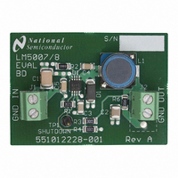
Manufacturer Part Number
LM5008EVAL
Description
EVALUATION BOARD FOR LM5008
Manufacturer
National Semiconductor
Specifications of LM5008EVAL
Main Purpose
DC/DC, Step Down
Outputs And Type
1, Non-Isolated
Voltage - Output
10V
Current - Output
300mA
Voltage - Input
12 ~ 95V
Regulator Topology
Buck
Board Type
Fully Populated
Utilized Ic / Part
LM5008
Lead Free Status / RoHS Status
Contains lead / RoHS non-compliant
Power - Output
-
Frequency - Switching
-
Other names
*LM5008EVAL


R
off-time set by this resistor must be greater than the maximum
normal off-time which occurs at maximum Vin. Using equation
2, the minimum on-time is 0.470 µs, yielding a maximum off-
time of 3.99 µs. This is increased by 117 ns (to 4.11 µs) due
to a ±25% tolerance of the on-time. This value is then in-
creased to allow for:
(400ns),
ance,
Using equation 3, R
The closest standard value is 267 kΩ.
D1: The important parameters are reverse recovery time and
forward voltage. The reverse recovery time determines how
long the reverse current surge lasts each time the buck switch
is turned on. The forward voltage drop is significant in the
event the output is short-circuited as it is only this diode’s
voltage which forces the inductor current to reduce during the
forced off-time. For this reason, a higher voltage is better, al-
though that affects efficiency. A good choice is an ultrafast
power diode, such as the MURA110T3 from ON Semicon-
ductor. Its reverse recovery time is 30ns, and its forward
voltage drop is approximately 0.72V at 300 mA at 25°C. Other
types of diodes may have a lower forward voltage drop, but
may have longer recovery times, or greater reverse leakage.
D1’s reverse voltage rating must be at least as great as the
maximum Vin, and its current rating be greater than the max-
imum current limit threshold (610 mA).
C1: This capacitor’s purpose is to supply most of the switch
current during the on-time, and limit the voltage ripple at Vin,
on the assumption that the voltage source feeding Vin has an
output impedance greater than zero. At maximum load cur-
rent, when the buck switch turns on, the current into pin 8 will
suddenly increase to the lower peak of the output current
waveform, ramp up to the peak value, then drop to zero at
turn-off. The average input current during this on-time is the
load current (300 mA). For a worst case calculation, C1 must
supply this average load current during the maximum on-time.
To keep the input voltage ripple to less than 2V (for this ex-
ercise), C1 calculates to:
Quality ceramic capacitors in this value have a low ESR which
adds only a few millivolts to the ripple. It is the capacitance
which is dominant in this case. To allow for the capacitor’s
tolerance, temperature effects, and voltage effects, a 1.0 µF,
100V, X7R capacitor will be used.
C4: The recommended value is 0.01µF for C4, as this is ap-
propriate in the majority of applications. A high quality ceramic
CL
The response time of the current limit detection loop
The off-time determined by equation 3 has a ±25% toler-
: When a current limit condition is detected, the minimum
t
OFFCL(MIN)
= (4.11 µs + 0.40µs) x 1.25 = 5.64 µs
CL
calculates to 264kΩ (at V
FB
= 2.5V).
11
capacitor, with low ESR is recommended as C4 supplies the
surge current to charge the buck switch gate at turn-on. A low
ESR also ensures a quick recharge during each off-time. At
minimum Vin, when the on-time is at maximum, it is possible
during start-up that C4 will not fully recharge during each 300
ns off-time. The circuit will not be able to complete the start-
up, and achieve output regulation. This can occur when the
frequency is intended to be low (e.g., R
case C4 should be increased so it can maintain sufficient
voltage across the buck switch driver during each on-time.
C5: This capacitor helps avoid supply voltage transients and
ringing due to long lead inductance at V
ceramic chip capacitor is recommended, located close to the
LM5008.
FINAL CIRCUIT
The final circuit is shown in Figure 13. The circuit was tested,
and the resulting performance is shown in Figure 6 through
Figure 8.
MINIMUM LOAD CURRENT
A minimum load current of 1 mA is required to maintain proper
operation. If the load current falls below that level, the boot-
strap capacitor may discharge during the long off-time, and
the circuit will either shutdown, or cycle on and off at a low
frequency. If the load current is expected to drop below 1 mA
in the application, the feedback resistors should be chosen
low enough in value so they provide the minimum required
current at nominal Vout.
PC BOARD LAYOUT
The LM5008 regulation and over-voltage comparators are
very fast, and as such will respond to short duration noise
pulses. Layout considerations are therefore critical for opti-
mum performance. The components at pins 1, 2, 3, 5, and 6
should be as physically close as possible to the IC, thereby
minimizing noise pickup in the PC tracks. The current loop
formed by D1, L1, and C2 should be as small as possible. The
ground connection from C2 to C1 should be as short and di-
rect as possible.
If the internal dissipation of the LM5008 produces excessive
junction temperatures during normal operation, good use of
the pc board’s ground plane can help considerably to dissi-
pate heat. The exposed pad on the bottom of the LLP-8
package can be soldered to a ground plane on the PC board,
and that plane should extend out from beneath the IC to help
dissipate the heat. Additionally, the use of wide PC board
traces, where possible, can also help conduct heat away from
the IC. Judicious positioning of the PC board within the end
product, along with use of any available air flow (forced or
natural convection) can help reduce the junction tempera-
tures.
IN
ON
. A low ESR, 0.1µF
= 500K). In this
www.national.com
Related parts for LM5008EVAL
Image
Part Number
Description
Manufacturer
Datasheet
Request
R

Part Number:
Description:
National Semiconductor [8-Bit D/A Converter]
Manufacturer:
National Semiconductor
Datasheet:
Part Number:
Description:
National Semiconductor [Media Coprocessor]
Manufacturer:
National Semiconductor
Datasheet:
Part Number:
Description:
Digitally Controlled Tone and Volume Circuit with Stereo Audio Power Amplifier, Microphone Preamp Stage and National 3D Sound
Manufacturer:
National Semiconductor
Datasheet:
Part Number:
Description:
Digitally Controlled Tone and Volume Circuit with Stereo Audio Power Amplifier, Microphone Preamp Stage and National 3D Sound
Manufacturer:
National Semiconductor
Datasheet:
Part Number:
Description:
AC97 Rev 2 Codec with Sample Rate Conversion and National 3D Sound
Manufacturer:
National Semiconductor
Part Number:
Description:
Manufacturer:
National Semiconductor
Datasheet:
Part Number:
Description:
Manufacturer:
National Semiconductor
Datasheet:
Part Number:
Description:
General Purpose, Low Voltage, Low Power, Rail-to-Rail Output Operational Amplifiers
Manufacturer:
National Semiconductor
Datasheet:
Part Number:
Description:
8-bit 20 MSPS flash A/D converter.
Manufacturer:
National Semiconductor
Datasheet:
Part Number:
Description:
Low Noise Quad Operational Amplifier
Manufacturer:
National Semiconductor
Datasheet:
Part Number:
Description:
Quad Differential Line Receivers
Manufacturer:
National Semiconductor
Datasheet:
Part Number:
Description:
Quad High Speed Trapezoidal? Bus Transceiver
Manufacturer:
National Semiconductor
Datasheet:
Part Number:
Description:
Dual Line Receiver
Manufacturer:
National Semiconductor
Datasheet:
Part Number:
Description:
TTL to 10k ECL Level Translator with Latch
Manufacturer:
National Semiconductor
Datasheet: